Бинарные наручные часы
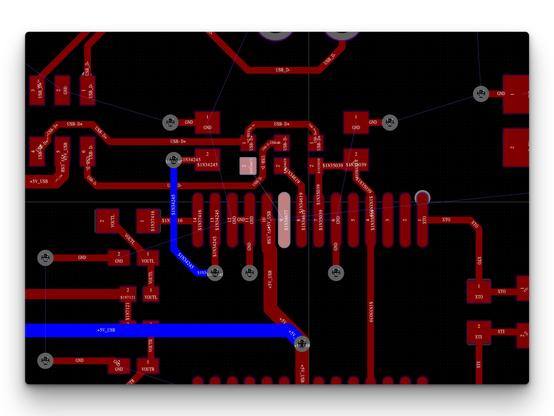
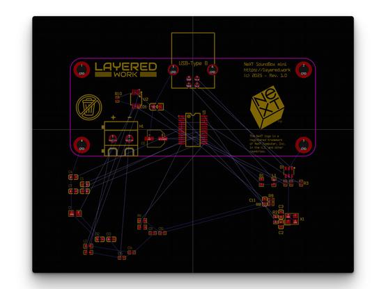
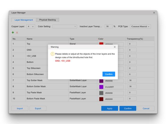
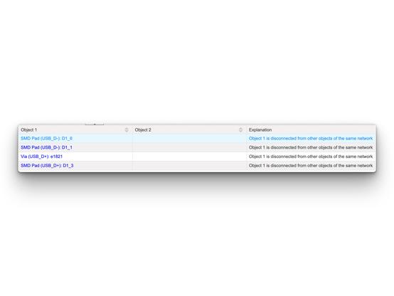
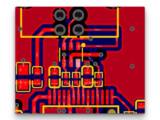
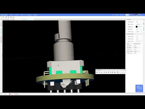
Я сделал наручные часы, которые показывают время четырьмя светодиодами в двоичном коде. Захотелось сделать подарок знакомому и заодно пройти весь цикл разработки embedded-устройства: схемотехника, четырёхслойная PCB, прошивка. В статье расскажу про решения, ошибки (включая ту, из-за которой USB не заработал) и устройство прошивки.
https://habr.com/ru/articles/1044176/
#atmega #arduino #arduino_c++_c #схемотехника #easyeda #электроника #pcb #rtc #часы
 👾
👾