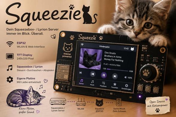
Squeezie – Squeezebox Server Remote Control
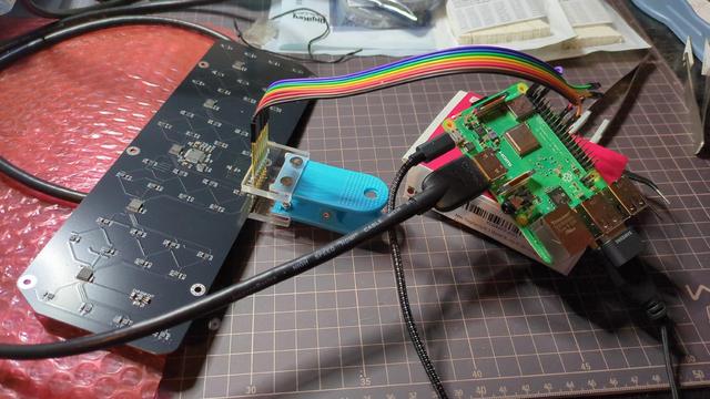
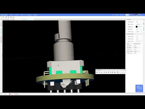
Mit „Squeezie“ entsteht ein ESP32-basierter Hardware-Controller für Lyrion bzw. klassische Squeezebox-Server — inklusive eigenem TFT-Display, individuell entwickelter Platine und natürlich jeder Menge Katzen
#AudioStreaming #diy #Embedded #ESP32 #HardwareProjekt #IoT #Lyrion #Maker #Mikrocontroller #Musikserver #Nerdstuff #OpenSource #PCBDesign #Squeezebox #Squeezer #TFTDisplay #WLAN
https://dirkwouters.de/squeezie-squeezebox-server-remote-control/