This Tiny Chip CHANGED EVERYTHING! - YouTube
The Stroy of the CMOS sensor and NASA.

This Tiny Chip CHANGED EVERYTHING! - YouTube
The Stroy of the CMOS sensor and NASA.
Z80 CPU Tester (Fail)
Recently I was watching Lee from More Fun Making|Fixing It with an “unpacking” video that contained a pile of Z80 CPUs ordered from a large Chinese supplier, and he was testing them using a neat Z80 CPU tester to work out if they were CMOS or NMOS devices and what frequency they would support.
I have a few Z80 CPUs kicking around, and not all nice new ones (that I was able to get from people like RC2014 and Small Computer Central) but random ones from a while back or more recently from online auction sites and so on, so thought it would be interesting to have a tester too.
I pretty found quickly found an open design that looked similar to the one in Lee’s video, but as I looked into the design, decided I didn’t really want to send off and pay for the larger PCB. Also the latest version of the tester I found has additional features that I’m not particularly interested in, so I thought I’d take the schematic and see if I could spin up my own version.
Spoilers: I made a wrong assumption and actually this is no good! But read on for the full tale of woe 🙂 Or just do what I ended up doing, and get yourself one of these: https://github.com/djtersteegc/z80-cmos-nmos-tester which is pretty much identical to the one used in the video!
There are a few “off the shelf” testers available from a number of places online, but they aren’t quite the same. This one from MyRetroStore looks like one of the easier ones to get and use: https://myretrostore.co.uk/product/z80-cpu-nmos-cmos-tester/ (Noting that this includes an ICSP header, I wonder if this is using a microcontroller. That was another thing I wondered about doing…)
The Original Design
I’m basing everything on the design from here: https://github.com/slabbi/Z80-CPU-Tester
This is using firmware for the Z80 that uses a lot of the information from this: https://github.com/skiselev/z80-tests
The basic idea of the original is that the board has a socket for the Z80, some ROM and RAM and IO decoding driving two sets of LEDs which give the status readout from the tests. The board also has a jumper-configurable clock which can select between 16MHz and 20MHz with divisors of 1,2,4,8,16. These all serve to allow the Z80 to boot and run a test program which uses some differences in undocumented features of the Z80 to determine which make of device it is and run it through its paces. Note, not everything is tested, but it will test basic instruction processing and IO.
The later V2 of the board also includes additional headers to break out the two IO ports and includes the option for IO input too.
The memory map is as follows:
0000-7FFFROM8000-FFFFRAMb1111 1110 (IO)IO PORT Ab1111 1101 (IO)IO PORT BKey components from the original design:
As I say though, the provided Gerber files present a neat design all ready to go, but on a 109×124 mm PCB. I want to see if I can get it into the magic 100×100 mm cheap PCB footprint.
My Z80 Tester Design
I don’t need the external IO features, so I can lose the 74LS573 and associated circuitry. This also means I can reuse the logic that has to decode IO reads, which also allows me to lose one of the three 74LS02s.
Pretty much everything else is the same. A0-A14 are routed to both ROM and RAM. D0-D7 are routed to both ROM and RAM, and the two IO ports via the two 74LS574s.
The address decoder logic is as follows.
The left-hand side signals come from the Z80 and the right-hand side signals go off to the memory or IO ports. CP0 enables PORT A and CP1 enables PORT B. The other signals are mapped as follows.
Z80 SignalsControl SignalDestinations/WRFrom this we can see that A15 selects between ROM and RAM (inverted to create /RAM_EN) and the memory read/write signals come from /MREQ and /RD or /WR respectively.
For the IO access, we can see that only /WR is supported and keyed into /IORQ. Then CP0 or CP1 are enabled depending on the state of A0 or A1 respectively. No other address decoding is performed for IO, so any values of A2 onwards are essentially irrelevant. I guess it is also possible to write to both ports at the same time using an address where both A0 and A1 are cleared (LOW).
The other piece of control logic worth noting is that the following signals on the Z80 are all pulled HIGH: /BUSREQ, /INT, /HALT, /WAIT.
/RESET and /NMI are also pulled HIGH but connected to a push button switch to allow them to be pulled LOW to activate them. I’ve used the circuits directly from the original here.
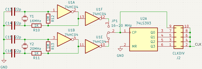
The clock circuit is again directly taken from the original:
This provides a jumper to select between 16MHz and 20MHz. It then passes through two inverters, presumably to clean it up, and then further jumpers to connect the output of the 4-bit binary counter to provide the actual used CLK signal.
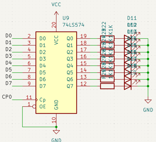
Here is one of the output PORTs connected to 8 LEDs.
We can see that this is triggered by CP0. PORTB is the same but triggered by CP1.
PORT A is used as an indicator that the tests are running. PORTB is used as an indicator for the type of Z80 CPU detected.
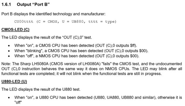
Here is the extract on decoding PORTB from the original Hardware (V2) English Manual:
The Big Fail
It turns out that removing the INPUT was based on a wrong assumption.
It wasn’t clearly documented that I could find initially, but after following some links from some links from a readme as part of researching this blog, I found the original code that everything is based on (here).
It turns out that the CMOS/NMOS detection relies on an undocumented OUT (C), 0 instruction. This can be hard-coded into the assembly with the line:
defb $ed, $71Which will force the unrecognised “OUT (C), 0” instruction to appear in the code. This apparently will output $00 for an NMOS device and $FF for a CMOS device. This has to be read back via a subsequent IN instruction to see what kind of chip is present.
Here in lies the problem. Without an IN device containing the latched output value, this won’t work. Sigh.
The original circuit uses a 74ALS990 read-back latch, which is quite hard to come by. The second version uses the combination of 74LS573, 74LS574 and transistors.
At this point I went off to the other circuit I discovered here: https://github.com/djtersteegc/z80-cmos-nmos-tester
As full design files are available for this one, and the PCB is withing the fabled 100×100 mm size, at this point I abandoned my own attempt and just got some of these boards ordered!
Further Thoughts
Seeing as I have some boards on the way though, I am pondering possible ways to get some use out of them. As the key undefined behaviour we’re interested in, is an OUT instruction, I’m now pondering if a sequence like:
LD C, 0With some appropriate delays, might be possible. As C is the address for the PORT driving the LEDs, then this would have the effect of flashing them twice for NMOS or flashing three times for CMOS.
Of course it renders the CMOS indicator itself LED useless. But I think this might work as an indicator, so this is one to test when the boards come back.
Someone Else’s Working Design
I’m still deciding if it is worth spending any more time on my board – either attempting to get the one I’ve now received working, or just redesigning a V2.
In the mean time, I’ve built up the existing one, which is a lot simpler design:
This works by flashing a number of times to indicate the type of Z80 – 1 flash for NMOS, 2 for CMOS and 3 for a U880. So as there is no INPUT readback, this must be doing exactly what I was pondering above – a sequence of OUT instructions, some of which will illuminate the LEDs (for a CMOS chip) and some of which won’t (for NMOS).
On passing a number of cheap Z80’s (all marked as Z84C0020PEC – yeah right ;)), I’ve ended up with most being NMOS, but running at least up to 8MHz, and two being CMOS. Two don’t seem to run at any frequency, so I’m guessing they are dead on arrival.
At present, I don’t have a 16MHz and 20MHz crystal, so I’m only testing up to 10MHz for now.
Conclusion
There is always a danger when modifying designs that something isn’t fully appreciated. And it gets worse with designs that are respins of earlier designs, and in this case that was a respin of yet another.
I often find that some of these projects that are widely used are often based on design decisions that seem lost in the mists of time. Or at least the depths of a random forum somewhere.
Anyway, this was one case where I was only considering the hardware as it appeared and not why it might have been the way it was. Oh well. All I’ve lost is an afternoon’s fun designing a board and around £5 on a PCB that will probably be useless once it arrives.
Ironically if I’d started this post prior to sending, I would almost certainly have found the error. As it happens, I started writing this a few hours after hitting “upload” and the erroneous board is now already in production! One day I’ll learn this lesson 🙂
Still on the plus side, the other board was only following on a few hours behind.
Kevin
#cmos #logic #nmos #pcb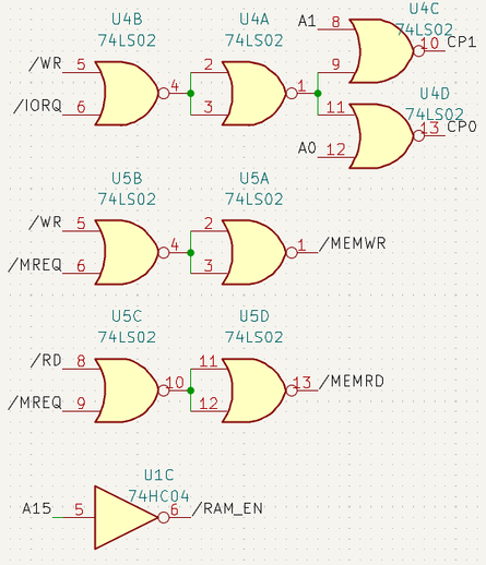
⚠️ Sony confirmed a one‑time online licence check for PlayStation purchases, you don't have to reconnect every 30 days, one verification is enough.
The 13.20 update for PS5 added a 30‑day timer to games bought after mid‑April 2026. If the console stays offline or the internal CMOS battery dies, the licence can drop and won't run until you verify online. Sony didn't explain why; players point to PIRACY countermeasures and fixes for refun...


Just designed a 3D printed lens system holder for a 6.5x6.5mm lens system that frames the 120Hz SVGA CMOS camera sensor (NOIP1SE0480A). This lens system is planned to be at the tip of a pen-like stylus for a blind person to feel visual art through a haptic interface.
https://codeberg.org/bcecoop/bce-noip1se0480-frame
#blind #maker #lenssystem #lens #cmos #sensor #3dprint #3dprinting #a11y #accessibility #accessible #bce #bcecoop #fosh #foss #freehardware
Submitted 6 new PCB (Printed Circuit Board) designs for manufacturing, including a 120Hz SVGA CMOS Camera board with FPC connector to a prototyping support board, an FPGA prototyping board, along with 3 new voltage regulated power supplies, including a 5V boost converter and 2 buck converters for 1.8V and 1.2V supplies.
https://bce.center/news/new-designs-120hz-svga-camera-power-supplies
#blind #maker #fosh #foss #freehardware #bce #pensee #pcb #ee #a11y #accessible #accessibility #bcecoop #fpga #camera #cmos #powersupply


Intel y QuTech ya producen cúbits semiconductores con procesos industriales (98% rendimiento). GlobalFoundries y Quantum Motion buscan chips cuánticos CMOS en 12/22 nm sin rehacer fábricas. https://aidoo.news/noticia/Wd0044
Intel y QuTech ya producen cúbits semiconductores con procesos industriales (98% rendimiento). GlobalFoundries y Quantum Motion buscan chips cuánticos CMOS en 12/22 nm sin rehacer fábricas. https://aidoo.news/noticia/Wd0044