If you want to understand quaternions better, try this amazing guide: https://eater.net/quaternions
#math #maths #mathematics #quaternions #modernalgebra #algebra #abstractalgebra #computergraphics #beneater
If you want to understand quaternions better, try this amazing guide: https://eater.net/quaternions
#math #maths #mathematics #quaternions #modernalgebra #algebra #abstractalgebra #computergraphics #beneater
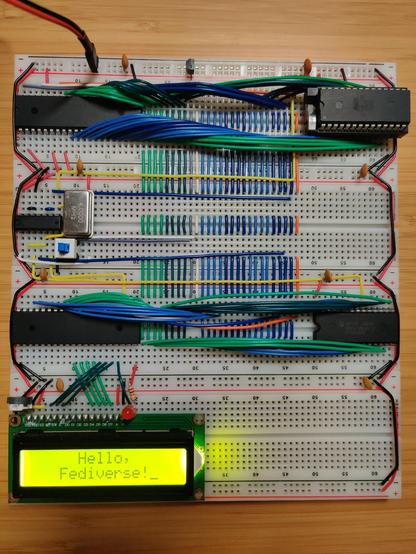
Reorganized my BE6502 breadboard computer
My main project has been paused while I waited for a shipment of components. Who knew I would need an XNOR gate IC?
In the meantime I switched back to working through Ben Eater’s videos on the 6502. I’m up to the ones on implementing the PS/2 keyboard interface. Before getting too far into it, I decided it was finally time to clean up the layout of the computer’s components. Ben’s layout, while compact, is also pretty messy. The address and data buses wind all over the place, making them difficult to understand and access for diagnostics or expansion. Also when I first built it I hadn’t bothered to take any power rails off of the boards before connecting them together, so my power rails were doubled up:
Inspired by some layouts that I’d seen on r/beneater, I went with a layout that has all the bus lines running vertically through the center of each board. Components are placed on the sides and connect to the bus lines instead of directly to each other. There are 27 bus lines:
There’s just enough room on the left side for the DIP40 ICs. The DIP28s go on the right, with a few columns to spare. Since the data bus starts at column 21, it aligns nicely with the numeric labels on the breadboard. The 1st data line is at column 21, 2nd line is at 22, 3rd at 23, and so on. I put the reset and clock lines in between the data and address busses in order to maintain this pattern for the address lines: 1st at 31, up to 16th at 46. I guess I could have gotten 0-based indexing instead of 1-based if I had put the DIP40s on the right side, but the 6502 really wants to be on the left side due to its pin layout.
I also did some creative wiring in order to fit the reset button below the oscillator so that it wouldn’t take up any extra real estate:
The center pins of the button share a column with the GND pin of the oscillator. The left pins are in the unusable space between the oscillator and the NAND IC. The right pins are in an otherwise unused column that runs underneath the oscillator. Since the reset button doesn’t take up any extra space, there’s room for an additional DIP14 next to the oscillator, and another two DIP14s or DIP16s to the right of the bus on that board.

This is awesome. The amount of anticipation I felt watching a man methodically work to get a breadboard computer to play a SID tune was ridiculous.
So #BenEater went the lengthy and roundabout route of prompting an LLM to output a Python program for creating a hex listing in a particular format, rather than just reading the manual page for the hexdump tool that xe was already using and learning its -e option.
The -e option actually takes the very same format specifiers that the Python script ended up with, and there's an example in the EXAMPLES section of the hexdump manual that gets one most of the way there.
One can do things the easy way by reading the doco, or the hard way with "AI" and #VibeCoding.
https://youtube.com/watch?v=LSMQ3U1Thzw&t=1626s
hexdump -e '"%04_ax: " 16/1 "%02X " "\n"' a.out

I don't know if folks are aware of this sweet lil #HomeBrew relay computer project being developed by #DiPDoT on #YouTube but here's their latest cool upload.
https://www.youtube.com/watch?v=BchBTWFFl-U
#Relay #Relays #RelayComputer #RelayProcessor #BreadBoard #TapeStorage also #BenEater fans should enjoy this.

Mais um dia de passagem do garbage collector
https://retropolis.com.br/2025/05/19/mais-um-dia-de-passagem-do-garbage-collector/
#MundoRetro #6502 #BenEater #CP437 #DEC #GarbageCollector #IBMPC110 #Intel80386 #KenShirriff #LLaMa2 #MicrosoftBASIC #MSDOS #PDP11 #RaymondChen #TCPIP #Venix

Clube do MS-DOS e assemelhados Raymond Chen fala de alguma coisa envolvendo a primeira década do Windows, já sabe, né? A gente para e lê. Agora, por exemplo, ele está falando dos usos dos ícones do moricons.dll, dos programas DOS que usam ícones no progman.exe e dos programas DOS que usam ícones no moricons.dll. Porque
I'm doing the thing that many nerds eventually do and building my own computer from the ground up with logic gates 😅.
Check out the first rambling post about WCPU-1 here: https://willwarren.com/2025/04/29/building-my-own-cpu-wcpu-part-1/