The Latest from RepRapMicron – Nail Gel, First Objects, and More
The Latest from RepRapMicron – Nail Gel, First Objects, and More
Teach your #microscope how to print: Low-cost rapid-iteration #OpenSource #microfabrication for #biology:
- no cleanroom required
- replace SU-8 #photoresist & silicon wafers by #3Dprinting #resin & microscope slides
- #fluorescence microscope-based maskless #photolithography
- achieve µm-scale precision across cm-sized areas
https://doi.org/10.1039/D5LC00181A
#DIYbio #lab #instruments #microfluidics
Teach your #microscope how to print: Low-cost & rapid-iteration #OpenSource #microfabrication for #biology:
-µm-scale precision across cm-sized areas
-no cleanroom requirement
-SU8 replacement
Preprint: https://doi.org/10.1101/2025.02.20.639256
GitHub: https://github.com/hinderling/fabscope
#DIYbio #lab #instuments #imaging #microfluidics #fabrication #3Dprinted
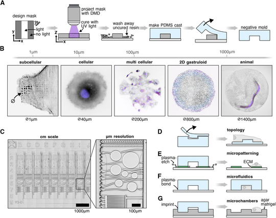
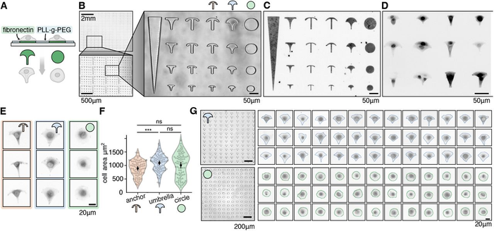

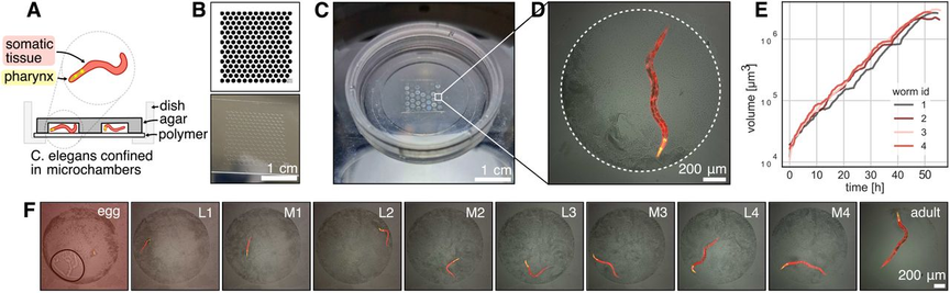

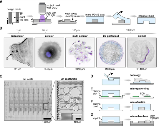
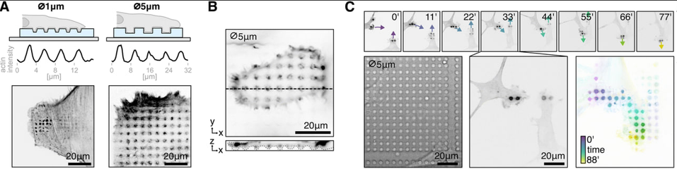
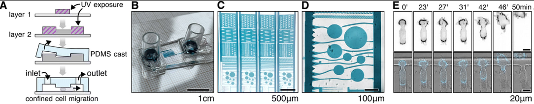
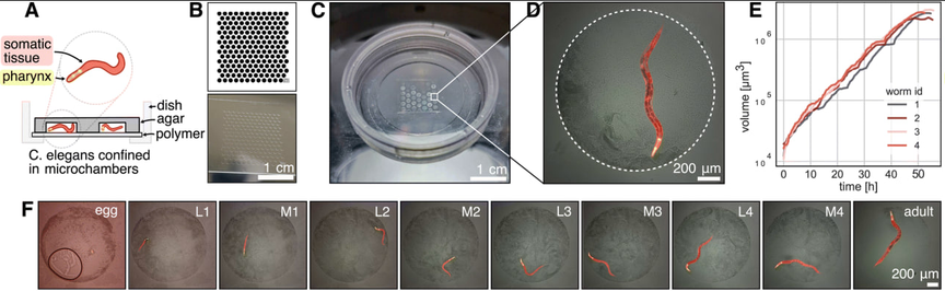
The application of traditional microfabrication techniques to biological research is hindered by their reliance on clean rooms, expensive or toxic materials, and slow iteration cycles. We present an accessible microfabrication workflow that addresses these challenges by integrating consumer 3D printing techniques and repurposing standard fluorescence microscopes equipped with DMDs for maskless photolithography. Our method achieves micrometer-scale precision across centimeter-sized areas without clean room infrastructure, using affordable and readily available consumables. We demonstrate the versatility of this approach through four biological applications: inducing cytoskeletal protrusions via 1 μm-resolution surface topographies; micropatterning to standardize cell and tissue morphology; fabricating multilayer microfluidic devices for confined cell migration studies; imprinting agar chambers for long-time tracking of C. elegans . Our protocol drastically reduces material costs compared to conventional methods and enables design-to-device turnaround within a day. By leveraging open-source microscope control software and existing lab equipment, our workflow lowers the entry barrier to micro-fabrication, enabling labs to prototype custom solutions for diverse experimental needs while maintaining compatibility with soft lithography and downstream biological assays. ### Competing Interest Statement The authors have declared no competing interest.
Postdoc - Acoustofluidic Platforms for Automated Sorting of Synthetic Cells
TU Delft
See the full job description on jobRxiv: https://jobrxiv.org/job/tu-delft-27778-postdoc-acoustofluidic-platforms-for-automated-sorting-of-synthetic-cells/?feed_id=88008
#acoustics #microfabrication #microfluidics #ScienceJobs #hiring #research
https://jobrxiv.org/job/tu-delft-27778-postdoc-acoustofluidic-platforms-for-automated-sorting-of-synthetic-cells/?feed_id=88008
Been working on some electrode patterns, starting to get some nice results. 🥳
Edges are a bit fuzzy/burry since I'm sputter depositing rather than something more line-of-sight like thermal evap. Getting a better dep method is high on the todo list.
Resist stack is an MMA/PMMA bilayer, substrate is silicon + ~100nm CuO, and electrodes are 150nm of aluminum via lift-off.
In theory, these should act as metal-semiconductor-metal photodetectors. Unsure if my test gear is sufficient though, might need to upgrade my electronics a bit. We'll see! 🤞


RT @uni_lu: 📣 #uni_lu researcher receives the first European Innovation Council (@EUeic) grant in Luxembourg for the REMAP project which aims to make #microfabrication sustainable.
#Sustainability
@unige_en @CNRS @NCSR_Demokritos @RINA1861
https://wwwen.uni.lu/university/news/slideshow/university_researcher_receives_the_first_eic_grant_in_luxembourg
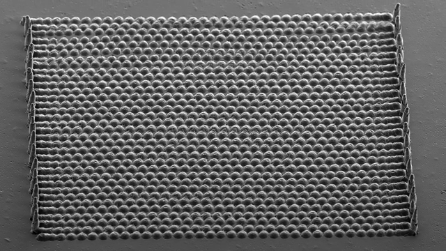
Getting a Fly’s-Eye View with Microfabricated Lens Arrays
Atomic force microscopy, laser ablation, and etching with a witches brew of toxic chemicals: sounds like [Zachary Tong] has been playing in the lab again, and this time he found a way to fabricate arrays of microscopic lenses as a result.
Like many of the best projects, [Zach]'s journey into micro-fabrication started with a happy accident. It happened while he was working on metal-activated chemical etching (MACE), which uses a noble metal catalyst to selectively carve high-aspect-ratio features in silicon. After blasting at a silver-coated silicon wafer with a laser, he noticed the ablation pits were very smooth and uniform after etching. This led him to several hypotheses about what was going on, all of which he was able to test.
The experiments themselves are pretty interesting, but what's really cool is that [Zach] realized the smooth hemispherical pits in the silicon could act as a mold for an array of microscopic convex lenses. He was able to deposit a small amount of clear silicone resin into the mold by spin-coating, and (eventually) transfer the microlens array to a glass slide. The lenses are impressively small -- hundreds of them over only a couple hundred square microns -- and pretty well-formed. There's always room for improvement, of course, but for an initial attempt based on a serendipitous finding, we'd call it a win. As for what good these lenses are, your guess is as good as ours. But novel processes like these tend to find a way to be useful, and the fact that this is coming out of a home lab doesn't change that fact.
We find this kind of micro-fabrication fascinating. Whether it's making OLED displays, micro-machining glass with plasma, or even rolling your own semiconductors, we can't get enough of this stuff.
#parts #science #etching #hydrofluoricacid #mace #mems #metalassistecchemicaletching #microfabrication #molding #nitricacid #pdms #silcon #silcone #silicon