£20,000 ISA, fully used.
You are paying 0.9% all in. A cheaper mirror portfolio costs 0.3%.
The action: move it. The gap is 0.6% = £120 a year on £20k.
Reinvested at 5%, that £120 a year is over £1,500 in a decade.
£20,000 ISA, fully used.
You are paying 0.9% all in. A cheaper mirror portfolio costs 0.3%.
The action: move it. The gap is 0.6% = £120 a year on £20k.
Reinvested at 5%, that £120 a year is over £1,500 in a decade.
ISA-to-Pension Bridge: Retire Before 57 in the UK
You hit your FI number at 45 and your pension is locked until 57. Twelve years to fund without touching the pot. The wrapper most UK FIRE plans skip entirely.
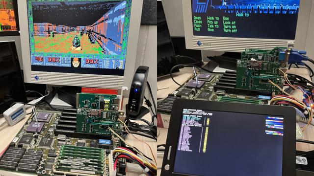
@charlotte @aens I hate to break it to you, but #Vortex86 chips are still newly being installed in #embedded #industrial setups as they are the only #SoC|s / #SOM|s in production with native #ISA support thus essential for a lot.of legacy systems that can't be replaved on a whim.
- And yes, the #Vortex86SX & #Vortex86DX are #i486-based.
And yes, I do want a minimalist #Linux for `i486`, WHICH IS WHY i started @OS1337 …
Preaching against the virgin birth, using the Bible as evidence? That's a new one.
The Bible most definitely says Mary was a virgin when Gabriel, the archangel, visited her to declare she was chosen to give birth to the Son of God. He was called Emmanuel, meaning God with us, and named JESUS.
Matthew 1:18-23
Luke 1
Isaiah 7:14
Even the Muslim Quran says Jesus (Isa) was born of the virgin Mary.

RE: https://social.ahlroos.me/@yle_fi_bot/116706902699466534
<3 Kniif <3
Ollaan tunnettu Knipin kanssa ysäriltä asti, josta osan aikaa #Knipi oli naapurinsetä.
Vähän on kyllä ikävä aikaa, että häneen ja ihanaan frouvaansa tämän tästä törmäsi.
#musiikki #muusikko #kuvataide #taide #kulttuuri #taiteilija #elokuva #leffa #näyttelijä #malli #kulttuurielämä #isä #isäsuhde #isyys #kuolema #menetys #vanhemmat #vanhemmuus #muistot #lapsuusmuistot #musadontti
I feel like overlapping FP and integer register file and ports may be better than overlapping FP with SIMD.
Because you kind of want scalar FP to be higher issue and lower latency that you need for SIMD float operations.
If you have 128-bit SIMD the goals are mostly aligned, but for >=256-bit sharing FP with SIMD becomes less attractive in my mind.
This also isn't all that relevant if your integer execution isn't something like 6 wide or wider.
It also gives you have more control over FP32 and FP64. Maybe you put FP32 on all ALUs, but FP64 only on the ones that also support IMUL (if you can share that logic).
Modern Graphics Via DisplayLink For Your ISA-Era PC