Arduino and AY-3-8910 – Part 3

I suggested in Part 2 that it might be possible to do some simple modulation of the amplitude of the AY-3-8910 channels rather than drive frequencies directly. This is taking a look at the possibilities of some kind of lo-fi direct digital synthesis using that as a basis.

https://makertube.net/w/uCSiBG5RBufGqspoHMYFPt

Warning! I strongly recommend using old or second hand equipment for your experiments.  I am not responsible for any damage to expensive instruments!

These are the key tutorials for the main concepts used in this project:

If you are new to Arduino, see the Getting Started pages.

Parts list

  • Arduino Uno.
  • AY-3-8910 chip.
  • Either GadgetReboot’s PCB or patch using solderless breadboard or prototyping boards.
  • 5V compatible MIDI interface.
  • Jumper wires.

Direct Digital Synthesis on the AY-3-8910

I’ve talked about direct digital synthesis before, so won’t go into full detail again. For more, see Arduino R2R Digital Audio – Part 3 and Arduino PWM Sound Output.

But the top-level idea is to set the level of the signal according to a value in a wavetable. If this value is updated at a useful audio rate then it will be interpreted as sound.

There are some pretty major limitations with attempting to do this on the AY-3-8910 however. The biggest one being that there are only 15 levels for the output on each channel.

So I’ll be working to the following properties:

  • 4-bit resolution for the output.
  • 8-bit wavetable.
  • 8.8 fixed point accumulator to index into the wavetable.
  • 8096 Hz sample rate.

YouTuber https://www.youtube.com/@inazumadenki5588 had a look at this and showed that the AY-3-8910 needs to be set up as follows:

  • Frequency value for the channel should be set to the highest frequency possible.
  • All channels should be disabled.

This is due to comments in the datasheet stating that the only way to fully disable a channel is to have 0 in the amplitude field.

Note: for a 8192 sample rate, that means writing out a sample to the AY-3-8910 registers approximately once every 124uS. With a 256 value wavetable, it takes almost 32 mS to write a complete cycle at the native sample rate, which would be around a 30 Hz output.

I’m not sure what the largest increment that would still give a useful signal might be, but say it was 8 values from the wavetable, then that would make the highest frequency supported around 1kHz. Not great, but certainly audible, so worth a try.

Setting up for DDS

I want a regular, reliable, periodic routine to output the levels from the wavetable, and the usual way to achieve this is using a timer and interrupt. As Timer 1 is already in use to generate the 1MHz clock for the AY-3-8910, I’m going to be configuring Timer 2 as follows:

  • Timer 2 is an 8-bit timer.
  • Use prescalar of 32 which gives a 500kHz clock source (16MHz/32).
  • Use CTC (clear timer on compare) mode.
  • Generate a compare match interrupt.
  • Do not enable any output pins.

The appropriate ATMega328 registers to enable this are:

// COM2A[1:0] = 00 No output
// WGM2[2:0] = 010 CTC mode
// CS2[2:0] = 011 Prescalar=32
ASSR = 0;
TCCR2A = _BV(WGM21);
TCCR2B = _BV(CS21) | _BV(CS20);
TCNT2 = 0;
OCR2A = 60;
TIMSK2 = _BV(OCIE2A);

Although it is worth noting that enabling OC1A can be quite useful for debugging. The following toggles the OC2A output (on D11) every time there is a compare match. The frequency seen on D11 will thus be half the anticipated sample frequency.

pinMode(11, OUTPUT);
TCCR2A |= _BV(COM2A0); // COM2A[1:0] = 01 for OC2A toggle

And this does indeed generate a signal. Here is a trace showing a timing GPIO pin and the AY-3-8910 output.

The problem is that this is meant to be a 440Hz sine wave, and whilst the shape isn’t too bad (it is a little distorted as the amplitude isn’t a true linear shape), the frequency is much nearer 100Hz than 440.

Analysis of Performance

The clue is the other trace, which is a timing pin being toggled every time the Interrupt routine is called. This is showing a 1kHz frequency, which means the IRS is being called with a 2kHz frequency rather than the anticipated 8192Hz. Curiously though I am getting an accurate 4kHz toggle on the timer output pin OC1A indicating the timer is correctly counting with a 8kHz frequency.

No matter how I configured things, the interrupt routine just would not do anything at a faster rate. I had to drop the frequency right down to 2kHz to get the output pin and interrupt routing running together. This means that something in the interrupt routine seems to be taking ~ 450uS to run.

After a fair bit of prodding and probing and checking the ATMega328 datasheet and double checking the register values, I have to conclude that the AY3891x library is just too slow at updating the registers for it to be able to run from the interrupt routine at this speed.

Taking a look at the register write() function in the library, which I need to use to update the channel level, I can see the following is happening:

void AY3891x::write(byte regAddr, byte data) {
latchAddressMode(regAddr);
daPinsOutput(data);
noInterrupts();
mode010to110();
mode110to010();
interrupts();
daPinsInput();
}

void AY3891x::latchAddressMode(byte regAddr) {
mode010to000();
daPinsOutput(_chipAddress | regAddr); // Register address is 4 lsb
mode000to001();
mode001to000();
mode000to010();
}

void AY3891x::daPinsOutput(byte data) {
byte i;

for (i = 0; i < NUM_DA_LINES; i++) {
if (_DA_pin[i] != NO_PIN) pinMode(_DA_pin[i], OUTPUT);
}

for (i = 0; i < NUM_DA_LINES; i++) {
if (_DA_pin[i] != NO_PIN) {
digitalWrite(_DA_pin[i], data & 0x01);
data = data >> 1;
}
}
}

void AY3891x::daPinsInput() {
byte i;

for (i = 0; i < NUM_DA_LINES; i++) {
if (_DA_pin[i] != NO_PIN) pinMode(_DA_pin[i], INPUT);
}
}

And every one of those modeXXXtoYYY() functions is a call to digitalWrite(), so I make that 22 calls to ditigalWrite() in order to write a single register value, plus around 16 calls to pinMode(). There are also 5 loops each looping over 8 values.

One person measured the Arduino Uno digitalWrite() function and concluded that it takes 3.4uS to run, so that is a minimum of 75uS of processing in every run through the interrupt routine just for those calls alone. That doesn’t include the calls and other logic going on. It could easily be more than twice that when everything is taken into account.

Dropping in some temporary pin IO either side of the call to the AY write function itself, and I’m measuring just over 250uS for the register update to happen, and that is just for one channel. This means that anything with a period of that or faster is starving the processor from running at all.

Measuring the Basic Performance

At this point I took a step back and created a free-running test sketch to really see what is going on.

#include "AY3891x.h"

AY3891x psg( 17, 8, 7, 6, 5, 4, 3, 2, 16, 15, 14);

#define AY_CLOCK 9 // D9
void aySetup () {
pinMode(AY_CLOCK, OUTPUT);
digitalWrite(AY_CLOCK, LOW);

TCCR1A = (1 << COM1A0);
TCCR1B = (1 << WGM12) | (1 << CS10);
TCCR1C = 0;
TIMSK1 = 0;
OCR1AH = 0;
OCR1AL = 7; // 16MHz / 8 = 2MHz Counter

psg.begin();

// Output highest frequency on each channel, but set level to 0
// Highest freq = 1000000 / (16 * 1) = 62500
psg.write(AY3891x::ChA_Amplitude, 0);
psg.write(AY3891x::ChA_Tone_Period_Coarse_Reg, 0);
psg.write(AY3891x::ChA_Tone_Period_Fine_Reg, 0);
psg.write(AY3891x::ChB_Amplitude, 0);
psg.write(AY3891x::ChB_Tone_Period_Coarse_Reg, 0);
psg.write(AY3891x::ChB_Tone_Period_Fine_Reg, 0);
psg.write(AY3891x::ChC_Amplitude, 0);
psg.write(AY3891x::ChC_Tone_Period_Coarse_Reg, 0);
psg.write(AY3891x::ChC_Tone_Period_Fine_Reg, 0);

// LOW = channel is in the mix.
// Turn everything off..
psg.write(AY3891x::Enable_Reg, 0xFF);
}

int toggle;
void setup() {
pinMode(11, OUTPUT);
toggle = LOW;
digitalWrite(11, toggle);
aySetup();
}

void loop() {
toggle = !toggle;
digitalWrite(11, toggle);
for (int i=0; i<16; i++) {
psg.write(AY3891x::ChA_Amplitude, i);
}
}

All this is doing is continually writing 0 to 15 to the channel A level register whilst toggling a GPIO pin. Putting an oscilloscope trace on the IO pin and the AY-3-8910 channel A output gives me the following:

This is running with a period of 6.96mS, meaning each cycle of 16 writes takes 3.5mS, giving me almost 220uS per call to the AY write function which seems to align pretty well with what I was seeing before.

And this is generating an audible tone at around 280Hz, so regardless of any timer settings or waveform processing, this is going to be the baseline frequency on which everything else would have to rest, which isn’t great.

Optimising Register Writes

So at this point I have the choice of attempting to write to the AY-3-8910 myself using PORT IO to eliminate the time it takes for all those loops and digitalWrite() calls. Or I could try some alternative libraries.

The library I’m using aims for the most portable compatibility: “This library uses the generic digitalWrite() function instead of direct port manipulation, and should therefore work across most, if not all, processors supported by Arduino, so long as enough I/O pins are available for the interface to the PSG.”

It is a deliberate design choice, but does require all three bus control signals to be used: BDIR, BC1, BC2.

Alternatives are possible with less pin state changes, but much stricter timing requirements. Some options include:

The following are projects that have not used a library, but just done their own thing:

Unfortunately none of these really solves the problem as the PCB I’m using does not neatly map onto IO ports to allow the use of direct PORT IO for the data.

So to improve things whilst using this same PCB will require me to re-write the library myself.

As a test however, it is possible to take the IO pin definitions used with the PCB and write a bespoke, optimised register write routine as follows:

void ayFastWrite (byte reg, byte val) {
// Mode=Addr Latch
digitalWrite(BC1, HIGH);
digitalWrite(BDIR, HIGH);

// Latch address
// NB: Addresses are all in range 0..15 so don't need to
// worry about writing out bits 6,7 - just ensure set to zero
PORTD = (PORTD & 0x03) | ((reg & 0xCF)<<2);
PORTB = (PORTB & 0xFE);
PORTC = (PORTC & 0xF7);

// Mode = Inactive
digitalWrite(BC1, LOW);
digitalWrite(BDIR, LOW);

delayMicroseconds(10);

// Mode = Write
digitalWrite(BC1, LOW);
digitalWrite(BDIR, HIGH);

// Write data
PORTD = (PORTD & 0x03) | ((val & 0xCF)<<2); // Shift bits 0:5 to 2:7
PORTB = (PORTB & 0xFE) | ((val & 0x40)>>6); // Shift bit 6 to 0
PORTC = (PORTC & 0xF7) | ((val & 0x80)>>4); // Shift bit 7 to 3

// Mode = Inactive
digitalWrite(BC1, LOW);
digitalWrite(BDIR, LOW);
}

I’m using the following mapping of data pins to Arduino digital IO pins to PORTS:

DA0-DA5D2-D7PORTD Bits 0-5DA6D8PORT B Bit 0DA7A3/D17PORT C Bit 3

To make this happen I have to ensure that the right bits are set to OUTPUTs and that BC2 is held HIGH prior to using the fastWrite function.

digitalWrite(BC2, HIGH);
DDRD |= 0xFC;
DDRC |= 0x04;
DDRB |= 0x01;

This now improves on that previous 280Hz and gives me 1600Hz performance.

So can I do any better? Well there are still between 6 and 8 calls to digitalWrite going on to handle the control signals…

#define BC1LOW {PORTC &= 0xFE;} // A0 LOW
#define BC1HIGH {PORTC |= 0x01;} // A0 HIGH
#define BC2LOW {PORTC &= 0xFD;} // A1 LOW
#define BC2HIGH {PORTC |= 0x02;} // A1 HIGH
#define BDIRLOW {PORTC &= 0xF7;} // A2 LOW
#define BDIRHIGH {PORTC |= 0x04;} // A2 HIGH

void ayFastWrite (byte reg, byte val) {
// Mode=Addr Latch
BC1HIGH;
BDIRHIGH;

// Latch address
PORTD = (PORTD & 0x03) | ((reg & 0xCF)<<2);
PORTB = (PORTB & 0xFE);
PORTC = (PORTC & 0xF7);

// Need 400nS Min
delayMicroseconds(1);

// Mode = Inactive
BC1LOW;
BDIRLOW;

// Need 100nS settle then 50nS preamble
delayMicroseconds(1);

// Mode = Write
BC1LOW;
BDIRHIGH;

// Write data
PORTD = (PORTD & 0x03) | ((val & 0xCF)<<2); // Shift bits 0:5 to 2:7
PORTB = (PORTB & 0xFE) | ((val & 0x40)>>6); // Shift bit 6 to 0
PORTC = (PORTC & 0xF7) | ((val & 0x80)>>4); // Shift bit 7 to 3

// Need 500nS min
delayMicroseconds(1);

// Mode = Inactive
BC1LOW;
BDIRLOW;

// Need 100nS min
}

The timings come from the AY-3-8910 datasheet:

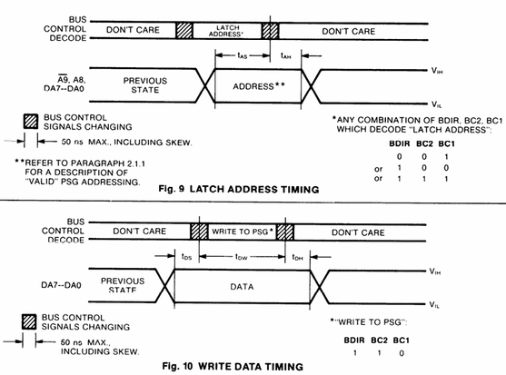
The actual minimum and maximum timings for the various “t” values are given in the preceeding table. Most have a minimum value, but tBD has to be noted: the “associative delay time” is 50nS. This means that any changing of BC1, BC2 and BDIR has to occur within 50nS to be considered part of the same action.

There is no means of having a nano-second delay (well, other than just spinning code), so I’ve just used a delayMicroseconds(1) here and there. This isn’t reliably accurate on an Arduino, but as I’m have delays of around half of that as a maximum it seems to be fine.

This now gives me the following:

This is now supporting a natural “as fast as possible” frequency of around 24kHz, meaning each call to the write function is now around 3uS. That is almost a 100x improvement over using all those pinMode and digitalWrite calls.

The downside of this method:

  • It is ATMega328 specific.
  • It is specific to the pin mappings and PORT usage of this PCB.
  • It does not support reading or other chip operations between the writes.

It is also interesting to see that the traces also show the high frequency oscillation (62.5kHz) that is being modulated regardless of the channel frequency and enable settings.

DDS Part 2

Success! At least with a single channel. This is now playing a pretty well in tune 440Hz A.

Notice how the frequency of the timing pin is now ~4.2kHz meaning that the ISR is now indeed firing at the required 8192 Hz.

Here is a close-up of the output signal. The oscilloscope was struggling to get a clean frequency reading, but this is one time I caught it reading something close! I checked the sound itself with a tuning fork (see video). It is indeed 440Hz.

Find it on GitHub here.

Closing Thoughts

I wanted to get something put together to allow me to drive a DSS wavetable over MIDI, with different waveforms, and so on, but it turned out to be a little more involved getting this far than I anticipated, so I’ll leave it here for now.

But hopefully filling in the gaps won’t take too long and will be the subject of a further post.

Now that I have something that works, I’m actually quite surprised by how well it is working.

Kevin

#arduinoNano #ay38910 #dds #define #directDigitalSynthesis #include #midi

Arduino and AY-3-8910 – Part 2

Following on from my initial experiments in Arduino and AY-3-8910 this post looks at the sound generation capabilities in a little more detail and adds some basic MIDI control.

https://makertube.net/w/3CxNBDKu5Gm6MQzMcLZYz6

Warning! I strongly recommend using old or second hand equipment for your experiments.  I am not responsible for any damage to expensive instruments!

These are the key tutorials for the main concepts used in this project:

If you are new to Arduino, see the Getting Started pages.

Parts list

  • Arduino Uno.
  • AY-3-8910 chip.
  • Either GadgetReboot’s PCB or patch using solderless breadboard or prototyping boards.
  • 5V compatible MIDI interface.
  • Jumper wires.

AY-3-8910 Sound Generation

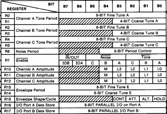
The most basic means of sound generation is to use the three tone generators to generate square waves at a frequency set using the on-chip registers (note in the following data from the datasheet, the R numbers are in octal – so there are 16 registers in total):

I don’t plan to get into the ins-and-outs of how to interface to the chip, instead I’ll link off to some excellent discussions here:

The frequency registers have a 12-bit resolution, spread over two 8-bit registers as shown below.

The datasheet tells us how to calculate the value to write to the register for a specific frequency:

  • Reg Value = System Clock / (16 * frequency)

For a 1MHz clock, the register value is thus 62500 / frequency, so the higher the frequency, the lower the register value. This means that concert A at 440Hz requires the value 62500 / 440 = 142, so:

  • R1 = 142 >> 8;
  • R0 = 142 & 0xFF;

For a 1MHz clock, the range of frequencies goes from 1MHz / 16 to 1 MHz / (16 * 4095) or ~62.5kHz to 15 Hz

The AY3891x library has a set of definitions that already defines the frequencies for each MIDI note from C0 to B8.

The volume for the note is set in another register:

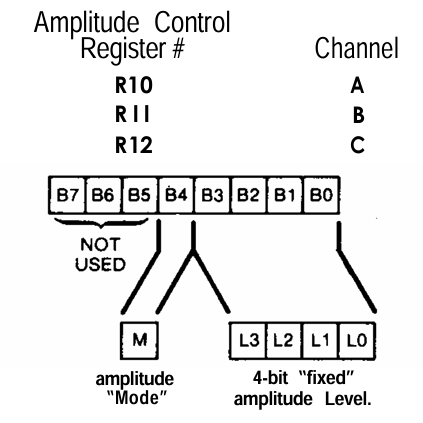
When Mode=0, the amplitude is set by the 4-bit fixed level. When Mode=1, the amplitude is controlled by the built-in envelope generator.

The envelope generator is a “global” setting for all channels, so for finer control, people often wrote their own envelope generator, manipulating the volume levels directly.

The datasheet describes the four parameters required to define an envelope:

Envelopes have a cycle time, which is set by R13 and R14 in a similar way to the frequency. This time the formula is:

  • Reg value = System Clock / (256 * env frequency)

Once again this is split over two registers, but this time supports a full 16-bit value.

There are graphical representations of what the combinations of the envelope bits mean, but I must confess I’m not entirely sure I understand them all and some don’t seem to sound, at least at the frequency I’ve chosen.

The Circuit

I’m reusing the PCB from GadgetReboot from Part 1, but this time I’ve added the button in (it is connected to A5 and GND) and added headers to the UART connection.

Unfortunately the UART only has GND, TX, RX – to use it with one of my Arduino MIDI Interfaces also requires a 5V connection, so I’ve taken that from the SD card header.

The Code

The note-playing code comes from the “AY3891x_EX3_Simple_Tone” example, including the ATmega328 specific code for the 1MHz clock. There is a table of note frequencies already provided for notes C0 through to B8, so it is just a case of mapping these onto MIDI notes C0 (12) through B8 (119).

One thing I wanted was to support simple polyphony using all three channels. But that means deciding what to do when a fourth note comes in – i.e. to ignore it or to replace one of the existing playing notes. I’ve left options for both.

I also wanted to make use of the channel volume too, so it is relatively trivial to map the MIDI 0..127 note velocity values onto the 0..15 levels for the sound generator. This is using the “fixed” level mode mentioned earlier.

But I also wanted the option to play with the envelopes, so I’ve wired in the button and have an option to use that to change between the different envelopes. As I’m not attempting anything particularly complex right now, I just gone with a fixed 10Hz frequency for the envelope generator’s cycle.

It won’t win any prizes for synthesis, but it does work.

Find it on GitHub here.

Closing Thoughts

Fundamentally, without the envelope generation this is the same as a three-channel Arduino tone() function, but at the time that was pretty ground-breaking as it allowed a system to keep playing a tone without having to keep driving it from the CPU.

Add in the noise channel, amplitude control and envelopes and you can start to see why this is also a step up musically too.

But when you get to making custom, per-channel envelopes, or even manipulating the 4-bit level control as a simple DAC or PCM generator, then you can start to see how some of the outstanding chiptunes of the time could be generated.

But even in this simple form there is still a fair bit more that could be done. Some examples might be:

  • Adding a potentiometer to control the envelope frequency. The when used with the triangle envelope this will act as a modulation control.
  • Add MIDI control values for the volume levels, modulation and choice of envelope.
  • Define some specific parameters to create “instruments” which can be selecting using MIDI program change messages.
  • Get the noise generator into the mix and define some percussion “instruments” too.

But what I really want to do is start taking a look at some of the sound drivers that were written that allow some of the chip tunes to come out.

I’m also getting to the point where I want my own PCB with things on it that I want to play with too.

Kevin

#arduinoNano #ay38910 #chiptunes #envelopeGenerator #midi

@fast_code_r_us I build this with (more for) my nephew with #arduinonano clone and an #SSD1306 128x32 #oled display.

I used the #U8g2 to display the text and the u8g2_font_unifont_t_weather to display the thermometer icon.

Arduino and AY-3-8910

I’ve had some AY-3-8910 programmable sound generators for a while and planned to do something with them, but they’ve sat in the “to think about” box for a while. But recently getting hold of the WhyEm sound card for the RC2014 has re-awakened my interest.

This is some “first looks” experiments with the AY-3-8910 and an Arduino.

  • Part 1 – Getting started and looking at playing YM files.
  • Part 2 – Adding basic MIDI control.
  • Part 3 – Basic experiments with direct digital synthesis.

https://makertube.net/w/26yAj7wAzZwCsFoBkJpZs2

Warning! I strongly recommend using old or second hand equipment for your experiments.  I am not responsible for any damage to expensive instruments!

These are the key tutorials for the main concepts used in this project:

If you are new to Arduino, see the Getting Started pages.

Parts list

  • Arduino Uno
  • AY-3-8910 chip
  • Either GadgetReboot’s PCB or patch using solderless breadboard or prototyping boards.

The AY-3-8910 PSG

The AY-3-8910 programmable sound generator is quite an iconic chip of its time. Not as popular maybe as the SID used in the Commodore 64, but still pretty widespread use in 8-bit computers of the time and apparently a number of arcade machines too.

There are a number of “compatible” chips, including the Yamaha YM2149. There is also the AY-3-8912 which is the same as the 8910 but without one of the general purpose IO ports, which take no part in the sound generation.

I’m not going to go into the details of the device itself, for that I’ll refer to the following resources:

The summary of the specification though is as follows:

  • Three square wave output channels.
  • Global AD envelope generator, with a selection of fixed envelopes.
  • Noise generator an option on the channels.
  • Mixer.

There is an 8-bit data register interface to the chip along with three control signals (BDIR, BC1 and BC2).

I should point out that it isn’t possible to buy new AY-3-8910 or YM2419 chips these days, so any that can be found online are almost certainly reclaimed from older hardware. These may or may not work reliably, but it will be a bit of a lottery.

There is a lot of discussion about the issue here: http://blog.tynemouthsoftware.co.uk/2023/01/testing-ay-3-8910-ym2149-sound-card-for-rc2014-and-minstrel-4D.html

This is why RC2014 eventually went with the “Why Emulator” approach: https://rc2014.co.uk/modules/why-em-ulator-sound-module/

Hardware

For once, I’m using someone else’s design for my initial messing about. There is a schematic and some hardware built on a protoboard shown in the Arduino YM3891x library here: https://github.com/Andy4495/AY3891x/tree/main/extras/hardware

But there is a PCB that was designed by GadgetReboot here: https://github.com/GadgetReboot/AY-3-8910. This can be ordered directly from PCBWay and so that is what I’ve used.

The only thing to watch out for, is that D2/D3 are reversed compared to the protoboard hardware. So whilst all other pin definitions in the library examples are fine, D2 and D3 need to be swapped to use them with the PCB.

I also didn’t bother to add the power LED (and R5), the toggle switch or the additional header pins.

The full pinout interface from the Arduino to the AY-3-8910 is as follows:

AY-3-8910ArduinoDA0-DA7D2-D8, A3BC1A0BC2A1BDIRA2CLOCKD9/RESETA4 (not used in the library)

The most critical one from a re-use point of view is the clock as the code uses the ATmega328P hardware Timer 1 to output a 50% duty cycle PWM signal on output OC1A (D9) to generate the 1MHz clock required by the AY-3-8910.

Using a different microcontroller will mean re-writing this part of the code for a suitable replacement timer.

The PCB also has the following Arduino GPIO pin use:

  • D0/D1 – UART pin header
  • D10-D13 – SD card pin header
  • A4 – /RESET of the AY-3-8910 but doesn’t appear to be required to use the library.

The AY-3-8910 is powered from the +5V from the Arduino. VIN for the Arduino is not connected, so USB power is assumed.

The Code

Taking the “AY3891x_EX3_Simple_Tone” example as a starting point, the following line needs updating as shown below:

// Original line
AY3891x psg( 17, 8, 7, 6, 5, 4, 2, 3, 16, 15, 14);

// Required for use with the PCB
AY3891x psg( 17, 8, 7, 6, 5, 4, 3, 2, 16, 15, 14);

This is using the “lesser number of pins” constructor, which assumes that the A8, A9, /RESET and CLOCK pins of the AY-3-8910 are not managed by the library. There is a more complete constructor to define the additional pins if required. There is a good description of how the AY-3-8910 interface works in the main source code: https://github.com/Andy4495/AY3891x/blob/main/src/AY3891x.cpp

I also switched any Serial.begin() statements to use 9600 baud for preference too.

With these changes, the simple tone example just works, as does the “AY3891x_EX8_Check_Orig_or_Clone”, which tells me I have an AY-3-8910 rather than a YM2149.

But what I really wanted was to play one of the tunes from a game I remembered. My first introduction to AY-3-8910 music was the 128K Spectrum version of The Neverending Story. This was one of the two games that came bundled with the original machine, and for someone used to the 48K beeps and boops it was an amazing upgrade.

Unfortunately I don’t seem able at present to find a “YM” file version of that tune to play, so instead I turned to a David Whittaker classic – “Glider Rider”. The “YM Jukebox” GitHub repository has a whole pile of YM files ready to use here: https://github.com/nguillaumin/ym-jukebox/tree/master/data/David%20Whittaker

There are (I believe) two key ways to get “chiptunes” for the AY-3-8910. A YM file is a stream of the register values sent to the chip to direct the sound generation. With one of these files, it is simply a case of turning these values into a C array and it can be included in an Arduino sketch (there are several steps required, see below, but it is all doable).

Another common way to get tunes is an “AY” file. As I understand things these are the actual Z80 assembler instructions required to drive the AY-3-8910 chip, so extracting the required data for use on another system is not so easy. These are really designed to be used on the original systems or via emulation.

To produce an Arduino source code file from a YM file requires the following steps (described here: https://github.com/Andy4495/AY3891x/tree/main/extras/tools):

python decoder.py GliderRider.ym force_interleavedpython bin2c14.py outputfile > chiptunes.h
  • Take the resulting const PROGMEM structure into the “chiptunes.h” file of the “AY3891x_EX6_Chiptunes_Flash” example sketch.

Note that due to the memory limitations of the Arduino Nano, the resulting C structure for the tune will have to be cut-off at around 2000 lines, but be sure to leave the termnating part of the structure:

const byte PROGMEM psg_data[] = {
0x6C,0x07,0x7C,0x07,0x7C,0x07,0x17,0x31,0x0F,0x00,0x00,0x00,0x00,0x20,
0x6C,0x07,0x7C,0x07,0x7C,0x07,0x1F,0x31,0x0D,0x00,0x00,0x00,0x00,0x00,
....
0x7C,0x07,0xBE,0x03,0x58,0x02,0x01,0x31,0x09,0x0E,0x00,0x00,0x00,0x00,
};

If there are build errors, then it might be because the structure is still too long. 2000 lines fits for me using around 97% of the programme memory of the Arduino Nano.

If full (longer) tunes are required, then the PCB has the option to hook up to an SD card and longer files can be stored there.

YM Files

Here is a little more detail about the above process required to get a YM file into C code, mostly for my own reference (the above links all talk about it pretty well tbh).

Step 1: A downloaded YM File is usually actually compressed using LHA. 7Zip can open these files and save the extracted version ready for step 2.

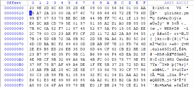
Here is the difference of the start of the files shown using a hex editor. Notice the “-lh5-” header near the start showing that this is a LHA compressed file, and a filename associated with the uncompressed version, in this case glrider.ym.

Uncompressed:

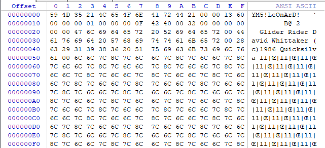
We can now clearly see he header information including the file identifier “YM5!” along with title, author and copyright information in comment fields.

The AU3891x library goes on to explain: “This uncompressed binary file has the audio programming registers stored in a non-interleaved format for more efficient compression. These values now need to be interleaved for more efficient playback.”

We can find more details of the YM file format here, in the words of the creator of the format, Arnaud Carré, directly: https://www.lynn3686.com/ym3456_tidy.html

A music-file is composed of YM2149 registers generated by the
original play-routine for each 50th seconds. As the YM2149 has 14 registers 8 bits each, that means 14 bytes for 1/50 second, so 700 bytes for one second of soundchip.

When I convert an ATARI music, I play the music on the ATARI, and I
store YM2149 registers set each 1/50sec (Vertical Blank time, VBL) in a big file as follow:

VBL1:
store reg0,reg1,reg2,...,reg12,reg13 (14 regs)
VBL2:
store reg0,reg1,reg2,...,reg12,reg13 (14 regs)
...
VBLn:
store reg0,reg1,reg2,...,reg12,reg13 (14 regs)

The problem is that is takes a lot of disk-space. Just count: A 10
minutes song will take 420000 bytes on disk. But don't panic, the music are compressed with LHARC method (using LHA program from Haruyasu Yoshizaki). To reach best compression ratio, I store registers in a different order:

VBL1 reg0, VBL2 reg0, VBL3 reg0 .... VBLn reg0
VBL1 reg1, VBL2 reg1, VBL3 reg1 .... VBLn reg1
...
VBL1 reg14,VBL2 reg14,VBL3 reg14.... VBLn reg14

Hence the “interleaved” format discussed previously. So looking at the file itself, specifically for YM5 it has the following format:

Offset Size Type Comment
0 4 DWORD ID of YM5 format. ('YM5!')
4 8 string[8] Check String ('LeOnArD!')
12 4 DWORD Nb of valid VBL of the file.
16 4 DWORD Song attributes (see below)
20 2 WORD Nb of digi-drum sample (can be 0)
22 4 DWORD YM2149 External frequency in Hz (ex:2000000 for ATARI-ST version, 1000000 for AMSTRAD CPC)
26 2 WORD Player frequency in Hz (Ex: 50Hz for almost player)
28 4 DWORD Vbl number to loop the song. (0 is default)
32 2 WORD Size (in bytes) of futur additinal data. (must be 0 for the moment)

So we can see this playing out from the above file:

00000: 59 4D 35 21 = "YM5!"
00004: 4C 65 4F 6E 41 72 44 21 = "LeOnArD!"
0000C: 00 00 13 60 = Number of frames: 4960
00010: 00 00 00 01 = Attributes:
b0: Set if Interleaved data block.
b1: Set if the digi-drum samples are signed data.
b2: Set if the digidrum is already in ST 4 bits format.
00014: 00 00 = No digidrum samples
00016: 00 0F 42 40 = External frequency 1MHz
0001A: 00 32 = Player frequency 50Hz
0001C: 00 00 00 00 = Number of loops for the song: 0
00020: 00 00

This header is then followed by:

For each digidrum sample:
4 DWORD sample size
nnnn BYTES sample data (8bits per sample)

NT-String Name of the song.
NT-String Name of the author.
NT-String Comments (YM file converter ?!)

All YM2149 registers.

4 DWORD End-File check. ('End!')

Which again we can now see in the uncompressed file:

(no digidrum samples)
00022: 476C6964657220526964657200 = "Glider Rider"
0002E: 4461766964205768697474616B657200 = "David Whittaker"
0003E: 2863293139383620517569636B73696C766100 = "(c)1986 Quicksilva"

00052: 6C6C7C8C... = 4960 values for reg0
013B2: 07070707... = 4960 values for reg1
...
0FC32: 02000000... = 4960 values for reg13
10F92: 00000000... = 2x4960 additional sets of values
13652: 45 6E 64 21 = "End!"

Curiously there seems to be data for 16 registers, which I guess would allow the inclusion of the two GPIO ports as well as the sound generation registers.

So to turn this into a stream of register values to send to the AY-3-8910 at a rate of 50Hz requires take the same “VBL” value for each register in turn and de-interleaving it.

This is the output from the decoder.py file as it processes the above:

Attempting to read file at glrider.ym...
YM5! format file detected based on first four bytes of file...
4960
File is interleaved...
Song title: Glider Rider
Author: David Whittaker
Comments: (c)1986 Quicksilva
Data length is 79360 bytes...
Song length is 4960 frames...
Deinterleaving...
Register 0: 0x6c 01101100
Register 1: 0x07 00000111
Register 2: 0x7c 01111100
Register 3: 0x07 00000111
Register 4: 0x7c 01111100
Register 5: 0x07 00000111
Register 6: 0x17 00010111
Register 7: 0x31 00110001
Register 8: 0x0f 00001111
Register 9: 0x00 00000000
Register 10: 0x00 00000000
Register 11: 0x00 00000000
Register 12: 0x00 00000000
Register 13: 0x20 00100000
==Frame#00000/04959======
Register 0: 0x6c 01101100
Register 1: 0x07 00000111
Register 2: 0x7c 01111100
Register 3: 0x07 00000111
Register 4: 0x7c 01111100
Register 5: 0x07 00000111
Register 6: 0x1f 00011111
Register 7: 0x31 00110001
Register 8: 0x0d 00001101
Register 9: 0x00 00000000
Register 10: 0x00 00000000
Register 11: 0x00 00000000
Register 12: 0x00 00000000
Register 13: 0x00 00000000
==Frame#00001/04959======

...

Register 0: 0x7c 01111100
Register 1: 0x07 00000111
Register 2: 0x54 01010100
Register 3: 0x00 00000000
Register 4: 0x0f 00001111
Register 5: 0x03 00000011
Register 6: 0x01 00000001
Register 7: 0x31 00110001
Register 8: 0x07 00000111
Register 9: 0x0c 00001100
Register 10: 0x0d 00001101
Register 11: 0x00 00000000
Register 12: 0x00 00000000
Register 13: 0x00 00000000
==Frame#04959/04959======

Notice that this is only pulling out the 14 sound generating registers. We can see this in the resultant de-interleaved file.

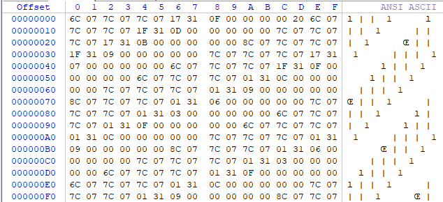
We can see tha tthe first two values correspond to the first items for reg0 and reg1: 6C and 07 and finish the 14 values with 20 before starting on the new set of 14 register values (again starting with 6C and 07 in this case).

The final step turns the above data stream into a C header file mentioned above.

To play the file thus requires the following algorithm:

Every 50Hz:
Read the next 14 register values from the data
Write all 14 register values out to the AY-3-8910

Closing Thoughts

I’ve really not done very much myself this time. The PCB was from GadgetReboot. The library from Andy4495. The tune data provided by the YM jukebox and all other scripts and bits of the process were available online.

Now I need to decide what I’d like to do with all this.

Kevin

#arduinoNano #ay38910 #chiptunes

Duppa I2C MIDI Controller – Part 3

This is a follow up post to Part 2 expanding on the code and adding in some of the alternative control options I mentioned.

  • Part 1 – getting to know the devices and testing them out.
  • Part 2 – adding MIDI to the LED ring and I2C encoder.
  • Part 3 – adding normal encoder, plain potentiometer, and endless potentiometer control.
  • Part 4 – revisits the idea with Waveshare Zero format devices and adds USB MIDI.

https://makertube.net/w/ncLFMqBwCUcrrM4r3mHJwd

Warning! I strongly recommend using old or second hand equipment for your experiments.  I am not responsible for any damage to expensive instruments!

If you are new to Arduino, see the Getting Started pages.

Parts list

  • Arduino Uno/Nano.
  • DuPPa small RGB LED Ring.
  • 10K potentiometer.
  • KY-040 rotary encoder module.
  • Bespoke hook-up wires (available from duppa.net).
  • Breadboard and jumper wires.

The Circuit

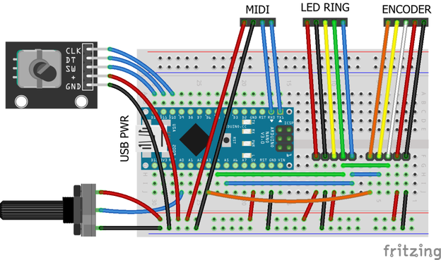
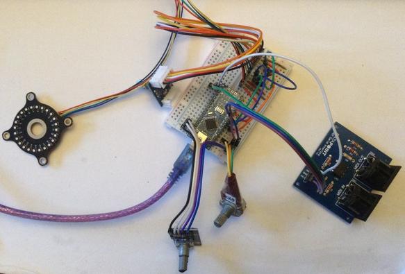
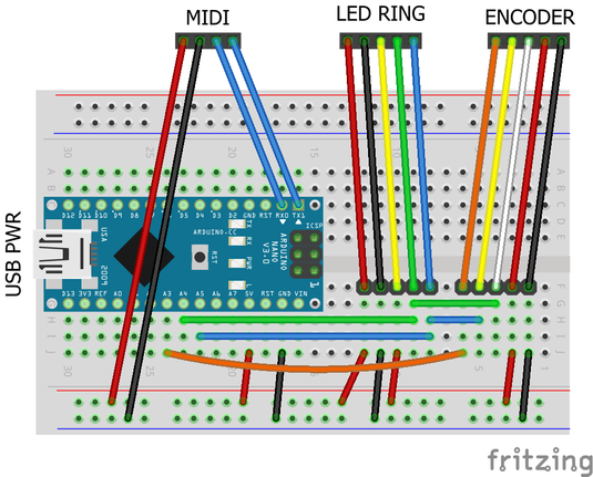
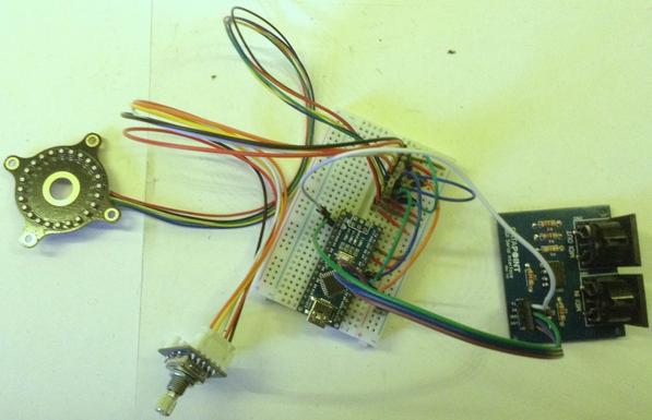
This circuit shows all three control options on the same diagram, but naturally use whichever one you require. There are the following three options:

  • Duppa I2C Encoder (from the previous project) on A4, A5 (SDA, SCL).
  • Plain potentiometer on A0.
  • Rotary encoder on D10, D11, D12.

In addition to the I2C LED Ring on A4, A5 (SDA, SCL) of course.

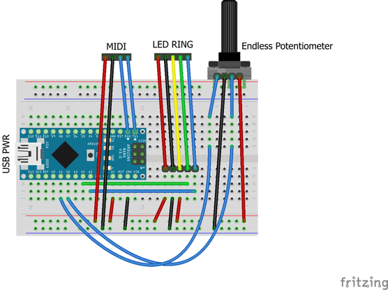
Here is a separate diagram for the endless potentiometer. I can be used alongside the above, but I’ve drawn it on its own for clarity.

Mine has the pins in the following order: Wiper A, GND, Wiper B, VCC.

The Code

This uses the code from Part 2 as a starting point and adds in some additional features.

The main aim is to add additional control options and then make them selectable in code. There are several definitions at the top of the file. One of them should be uncommented to enable that control option.

//#define CC_ENCODER
#define CC_POTENTIOMETER
//#define CC_I2CENCODER
//#define CC_ENDLESSPOT

Each control method will have some associated functions, but the interface will be hidden away behind these definitions and called from the main code, something like the following.

#ifdef CC_ENCODER
#include <librarycode.h>
... control specific definitions ....

void encSetup() {
// Control specific setup code
}

void encLoop() {
// Control specific loop code
}
#else
void encSetup() {}
void encLoop() {}
#endif

If that control option is not enabled, then it will just end up with the two empty functions.

Normal Potentiometer

This is fairly straightforward. I’m using the averaging technique I’ve mentioned before (details here) and include a counter so that the pot isn’t read on every scan, otherwise it slows down all other processing significantly.

The pot reading is scaled down to 7-bits from the default 10-bit value with a bitshift.

I’ve opted to have a jump if the CC value is updated over MIDI rather than anything more sophisticated, as that is probably the simplest.

All the same display options are available as used previously: one LED per CC; scaled to multiples of the ring size; or scaled to a single ring.

This works quite well with all of them, but probably makes most sense when the MIDI CC range is scaled to a single revolution of the LED ring.

CC_WRAP has no effect when used with a normal potentiometer, as the pot itself does not wrap around.

Rotary Encoder

This is using the same encoder library I’ve used before in my Arduino MIDI Rotary Encoder Controller. This makes the scanning code relatively straight forward.

I’ve refactored out the increment/decrement functions from the I2C encoder code into midiCCIncrement and midiCCDecrement, so these can now be used by both encoder options.

These encoder modules are often switched, but I’m not making use of the switch here.

Once again, all the same display options are available: one LED per CC; scaled to multiples of the ring size; or scaled to a single ring. CC_WRAP can be on or off.

Endless Potentiometer

There is a detailed discussion of how these work here: https://hackaday.io/project/171841-driveralgorithm-for-360-deg-endless-potentiometer
My initial thought was that I could just use one of the wipers, assuming it would go from 0 to full resistance and immediately back to zero, but they don’t – they gradually go from 0 to full resistance and then gradually back to 0 again. See the diagram in the above link.

This means that some processing is required to get a single reading out of them, so I ended up using a library from here:

Well actually, I ended up using the slight variant of the library as used on the “Ottopot” MIDI controller, which can be found here:

In my case I just dropping in the endlesspotentiometer.cpp/h files into my Arduino sketch (swapping any includes from <> to “” in the process). There was one reference to main.h that needed removing, and it required a definition of MAX_POT_VALUE which is 1023 for an Arduino Uno.

Then the code is fairly straight forward as the library is able to give an indication of direction and how much the pot has moved.

One thing to watch out for – I wanted this to be able to act on midiCC in a relative manner, replication the benefits of an encoder, but with a potentiometer, so I needed to know how much the pot had changed and then add that to the current midiCC value, rather than set it directly.

To do this I allowed midiCCIncrement/Decrement to take a parameter – how far to increase or decrease midiCC.

The core code for handling the endless pot was thus:

endpot.updateValues(epot1.avgeAnalogRead(PIN_EALG_1),
epot2.avgeAnalogRead(PIN_EALG_2));
if (endpot.isMoving) {
if (endpot.direction == endpot.CLOCKWISE) {
midiCCIncrement(endpot.valueChanged);
} else if (endpot.direction == endpot.COUNTER_CLOCKWISE) {
midiCCDecrement(endpot.valueChanged);
}
}

I also turned the potentiometer averaging code into a class of its own so I could also use it here for both analog readings of the endless pot.

It took a bit of experimentation with the sensitivity and threshold settings and how they interacted with the frequency of reading, but I’ve ended up with something that seems to work ok for me.

Summary

Although at the start I said that one of the options should be commented out to select it, in reality, if the devices are all on separate IO pins, then actually they can all be enabled at once.

And it does seem to work pretty well, with all four methods: I2C encoder, plain encoder, potentiometer – all interacting as you might expect they would.

Find it on GitHub here.

Closing Thoughts

I was quite surprised how usable everything was with all four input methods enabled. I probably wouldn’t recommend it for typical use, but it was a bit of fun.

It is particularly satisfying to sweep through the entire range using the pot with “one LED per CC” enabled, even though scaling a single ring to the potentiometers range makes more sense (to me).

At some point I will try to get several controls up and running.

Kevin

#arduinoNano #duppa #endlessPotentiometer #i2c #ifdef #midi #potentiometer #rgbLed #rotaryEncoder

Duppa I2C MIDI Controller – Part 2

This is a follow up post to Part 1 where I’m starting to look at MIDI applications and a range of control options. Part 1 – getting to know the devices and testing them out. P…

Simple DIY Electronic Music Projects

Duppa I2C MIDI Controller – Part 2

This is a follow up post to Part 1 where I’m starting to look at MIDI applications and a range of control options.

  • Part 1 – getting to know the devices and testing them out.
  • Part 2 – adding MIDI to the LED ring and I2C encoder.
  • Part 3 – adding normal encoder, plain potentiometer, and endless potentiometer control.
  • Part 4 – revisits the idea with Waveshare Zero format devices and adds USB MIDI.

Since posting the first part, I’ve stumbled across a rather excellent DIY MIDI controller that uses 8 of these Duppa LED rings and 8 endless potentiometers (which I hadn’t realised was even a thing!). It is a fantastic build, based on a Teensy and PlatformIO and I totally recommend going and taking a look. Read about it here: https://gerotakke.de/ottopot/.

https://makertube.net/w/2oKgvpZ29L2oExanSaUXjE

Warning! I strongly recommend using old or second hand equipment for your experiments.  I am not responsible for any damage to expensive instruments!

If you are new to Arduino, see the Getting Started pages.

Parts list

  • Arduino Uno/Nano.
  • DuPPa small RGB LED Ring.
  • Mini I2C Encoder.
  • Bespoke hook-up wires (available from duppa.net).
  • Breadboard and jumper wires.

The Circuit

I eventually want to include various options for controlling the ring and MIDI:

  • Duppa I2C rotary encoder.
  • Plain rotary encoder.
  • Simple potentiometer.
  • Endless potentiometer.

I don’t have any endless potentiometers yet, they are something I’ve only recently found exist, but I’ll post again when I get a chance to try them!

The required connections, naturally, are quite different for each case:

  • Duppa I2C encoder: connects to SDA/SCL.
  • Plain rotary encoder: requires two digital IO pins.
  • Simple potentiometer: requires a single analog input.
  • Endless potentiometer: requires two analog inputs.

In this first post, I’m just looking at the same Duppa I2C Encoder and LED Ring that I used in Part 1 but am adding a 5V compatible MIDI module.

The Code

Once again, this is using the Duppa Arduino library: https://github.com/Fattoresaimon/ArduinoDuPPaLib/

CC, Pots, Encoders…

The biggest issue I find with attempting to develop a MIDI CC controller is where is the authoritative definition of what the CC value actually is? What do I mean by that? Well we have the value in the synthesizer, defined on power up or via the on-board controls. And then we have the setting in the external MIDI controller. Until the MIDI controller sends an updated value to the synth, these will be different. And if the value on the synth changes locally, e.g. using knobs or controls on the synth, then they will be out of sync.

I’ve not found an easy answer to this, but what I’m planning is having the CC controller receive MIDI CC messages as well as send them. This means that if the CC value is changed directly on the synth, if the synth transmits that over MIDI, then it will be received by the external controller which can update its own value accordingly.

One problem with this is that there are two types of hardware controller: relative or absolute.

A rotary encoder is a relative controller – it turns in a direction and the value will increase or decrease accordingly. If the internal knowledge of the CC value changes, the encoder will just continue to increase of decrease from that new value instead.

A potentiometer is (usually) an absolute controller – it turns and has a value. If the internal knowledge of the CC value changes, then unless you have a motorised potentiometer, it will still be in the same place so on turning there will be a jump in value from the stored value to the new setting of the potentiometer.

One option to deal with absolute values is to have the new position value only become relevant once the turning “catches up” with the internal value and the starts adjusting it from that point onwards. But this can create a disjoint between the user experience of turning the knob and it actually changing anything. But on the plus side, absolute values are “remembered” when powered off – providing the knobs are left in the same place.

I’m hoping to use the encoders as a pseudo potentiometer. But it isn’t going to be possible to have a complete rotation considered the same as a full sweep of a potentiometer, as that will be down to the number of “detents” per rotation and that won’t be anything like enough to support 128 MIDI CC values. But I do plan to indicate the value by LEDS, and use those to indicate the position in the full sweep. This will allow the starting point to change if a CC message is received.

One solution to this problem, and that used by the Ottopot controller mentioned at the start, is to use an endless potentiometer. This not-only allows a variable starting position, but it also represents a full-sweep of values with a single turn as per a simple potentiometer.

So when I get hold of some of those I’ll come back to revisit this code.

For this first version there is code for the I2C encoder implemented using the following functions:

  • i2cEncSetup()
  • i2cEncLoop()
  • i2cEncIncrement()
  • i2cEncDecrement()

These are based on the code I used in Part 1. The increment and decrement functions act on a global “midiCC” directly, which stores the CC value to use using the range of a single MIDI “byte” 0 to 127. There is a compilation option to allow wrapping around (between 0 and 127) or not.

MIDI Handler

The Arduino MIDI library is used for both send and receive and all MIDI functionality is wrapped up in the following functions:

  • midiSetup()
  • midiLoop()
  • midiControlChange()

There are a few additional functions to give an optional LED indication of MIDI activity. Within the MIDI loop the midiCC value is checked and if it has changed then a MIDI control change message is transmitted:

void midiLoop() {
MIDI.read();
if (lastMidiCC != midiCC) {
MIDI.sendControlChange(MIDI_CC, midiCC, MIDI_CHANNEL);
}
}

There is an option to have software MIDI THRU enabled and this is handled as part of the MIDI.read() call. On setup midiControlChange() is installed as a handler function for MIDI CC messages and if the correct CC message is received on the correct MIDI channel then the midiCC value is updated directly.

One consequence of using midiCC directly and it being changed by either the encoder or from MIDI is that any change will also trigger the sending of the CC value out too.

This means that if MIDI THRU is enabled and a MIDI CC value is sent to the Arduino then it will almost certainly be sent back over MIDI twice – once as part of the THRU handling, and once as a consequence of it having changed the Arduino’s stored midiCC value.

LED Ring Indicator

The simplest implementation will be to scale the 24 LEDs of the ring to the 128 MIDI values and light up the LED that best represents the chosen value.

An alternative is to use one LED per MIDI CC value and allow the ring to loop round, possibly in a different colour. For 128 values across 24 LEDs this means there will be five full circles of the ring plus 8 more.

I’ve also provided the option to scale the MIDI CC values to a multiple of the LED ring so that the full MIDI 0..127 range wraps around back to 0 back at the start of the ring.

In the following, scalemax is the largest multiple of NUM_LEDS that will fit in 128, then the midiCC value is scaled to that new range and then used in the rest of the LED calculation.

int scalemax = 128 - 128 % NUM_LEDS;
int midiCC_scaled = (midiCC * scalemax / 128);
nextLed = midiCC_scaled % NUM_LEDS;
uint32_t col=0;
if (midiCC_scaled < NUM_LEDS) {
col = 0x00003F;
} else if (midiCC_scaled < NUM_LEDS*2) {
col = 0x003F3F;
} else if (midiCC_scaled < NUM_LEDS*3) {
col = 0x003F00;
} else if (midiCC_scaled < NUM_LEDS*4) {
col = 0x3F3F00;
} else if (midiCC_scaled < NUM_LEDS*5) {
col = 0x3F0000;
} else {
col = 0x3F003F;
}

One quirk to note is that the LEDs are numbered anti-clockwise, so at some point I’ll have to reverse the LED number when it comes to presenting an increasing CC value as a clockwise changing display.

I’d also like to have a bit of a lazy, dragging LED change, so I want to implement something that fades illuminated LEDs out as the value changes, leaving some kind of “tail” as the LED moves.

To do this, I’ve used an array to store the colour value used for any illuminated LEDs and then at regular intervals that colour is updated to fade back to OFF.

I’ve implemented a relatively simple fade – basically each of the R, G and B components of the colour is bit-shifted to the right by 1 on each “scan”. This has the effect of continually dividing the colour value by 2 until it reaches 0. The only thing to watch out for is that I don’t do this for the current illuminated LED.

Also note that I only pull out the most significant 7 bits of each 8 bit value (by & 0xFE) so that the shift doesn’t map the least significant bit of one value down into the next colour.

for (int i=0; i<NUM_LEDS; i++) {
if (i != nextLed && ledMap[i] > 0) {
uint32_t newcol = ((ledMap[i] & 0xFE0000) >> 1)
+ ((ledMap[i] & 0x00FE00) >> 1)
+ ((ledMap[i] & 0x0000FE) >> 1);
LEDRingSmall.LEDRingSmall_Set_RGB(i, newcol);
ledMap[i] = newcol;
}
}

All the LED handling is wrapped up in the following functions:

  • ledSetup()
  • ledLoop()
  • ledIndex()

The last function is responsible for swapping the LED numbers around to make them go clockwise. It isn’t as simple as doing NUMLEDS – led as I still want the first LED to be at “12 o’clock”, hence the function to return the correct index.

Find it on GitHub here.

Closing Thoughts

I am so pleased with that lazy LED change effect.

Having so many turns of the encoder isn’t particularly practical at the moment, but it does work. It is certainly good to have a few configuration options – especially the option to wrap around, as it takes quite a few turns to get from 0 to 127.

In a follow up post I’ll take a look at some of the other options, and when I get my endless encoders in the post that will definitely get a mention too.

I also want to wrap up the existing code somehow to allow for several LED CC controls if required and some kind of box might also be nice.

Kevin

#arduinoNano #duppa #i2c #midi #rgbLed #rotaryEncoder

Duppa I2C MIDI Controller – Part 1

I’ve had my eye on Duppa’s rather neat looking I2C LED rings and rotary encoders for some time and finally pushed “go” on getting a couple. I want to use them as the basis f…

Simple DIY Electronic Music Projects

EuroRack 6HP Arduino Mozzi Module – Basic VCO

This is the first project based on my EuroRack 6HP Arduino Mozzi Module. It is loosely based on HAGIWO’s Arduino Mozzi VCO Module.

https://makertube.net/w/hnocMAhYkajd8nX2vwuR2u

Warning! I strongly recommend using old or second hand equipment for your experiments.  I am not responsible for any damage to expensive instruments!

These are some previous posts for the main concepts used in this project:

If you are new to Arduino, see the Getting Started pages.

Parts list

The Circuit

This uses the EuroRack 6HP Arduino Mozzi Module with the pots and jacks assigned as shown below.

The four potentiometers control the following:

  • POT 1 – OSC 1 core frequency offset (from V/Oct CV).
  • POT 2 – OSC 2 frequency ratio OSC1.
  • POT 3 – Waveform for both oscillators: sine, triangle, saw, square.
  • POT 4 – Octave: 1 lower, normal, 1 higher, 2 higher.

There are three CV inputs:

  • V/Octave pitch.
  • OSC1 vs OSC2 gain.
  • Pitch modulation.

The Code

The code is inspired by that of HAGIWO’s Mozzi VCO, in that I’m using Mozzi with two oscillators, with multiple waveforms, and I’m using HAGIWO’s gain profile for CV. But I’ve added a few extras and have rewritten the core Mozzi code to hopefully be a little more optimal.

The main V/Oct calculation has to happen every scan and HAGIWO uses a look-up table in PROGMEM for the fractional voltages that correspond to each value of the ADC and then uses those in the standard Volts to frequency equation:

Freq = BaseFreq . 2^CV

For a 10-bit resolution (the resolution of the Arduino ADCs) this requires 1024 values across the whole 5V range. That equates to 4.8828mV per step (5/1024) and as full octave of 12 steps is 1V that equates to 83.3mV per semitone.

The various CV recommendations I’ve seen suggest using a BaseFreq equal to C4, which is 261.6256 Hz in the calculation unless it is for a LFO or clock in which case a BaseFreq of 2Hz is recommended – which corresponds to 120 bpm if used for a clock. The BaseFreq is the frequency used for 0V. Many analog synths will accept negative voltages to go lower, but as this is an Arduino it only supports 0V to 5V.

HAGIWO uses a table of float values and uses floating point arithmetic to work out the frequency. I’ve opted to use fixed point arithmetic and also rather than store the CV “step” values in the table have pre-calculated the whole 2^CV for each step.

Here is some Arduino code that will output the required look-up table values. My full version will first output the individual voltage steps to 6 decimal places; then for the float version of 2^CV; and finally for the fixed point 16.16 equivalent – that is 16 bits for the integer part and a fixed 16 bits for the binary equivalent of the decimal part.

The code below just does the last part. This is using the FixMath library which was written for use with Mozzi (more here).

#include <FixMath.h> // Designed for use with Mozzi

int res = 10; // 10-bit resolution
float maxv = 5.0; // Max voltage

void setup() {
Serial.begin(9600);

int max = (1<<res) - 1;
float cvstep = maxv / ((float)max+1.0);

Serial.print("\n\n");
Serial.print("Resolution=");
Serial.print(res);
Serial.print(" bits (0 to ");
Serial.print(max);
Serial.print(")\tV/step=");
Serial.print(cvstep,6);
Serial.print("\n");

float cv = 0.0;
for (int i=0; i<=max; i++) {
if (i%16 == 0) {
Serial.print("\n");
}
float freqpow = pow(2, cv);
UFix<16, 16> q16n16fp = freqpow;
Serial.print("0x");
Serial.print(q16n16fp.asRaw(), HEX);
Serial.print(",");
cv += cvstep;
}
}

void loop() {}

I’ve used this to create the q16n16 version of the 1024 values required to calculate the frequency for each of the 0..1023 values that the 1V/Oct analog input could provide, covering the full 5V range. This is stored in the header file v2voct.h that is part of the code.

This does mean that any calculation of frequency must be done using the FixMath 16.16 values, for example:

UFix<16,16> q16n16potfreq = mozziAnalogRead(POT1);

This code takes the unsigned integer value (0 to 1023) from mozziAnalogRead and automatically turns it into a 16.16 fixed point format value in variable q16n16potfreq – note that in each case the decimal part will be zero as the starting point is an integer between 0 and 1023.

When reading values in from the look-up table, they have to be pulled in “raw” as they are already in the 16.16 format. But as Arduino doesn’t know anything about this format, they have been declared as uint32_t values in the PROGMEM structure, but then need to be read back out and treated as 16.16 values as show below.

#define CVSTEPS 1024
static const uint32_t q16n16fp [CVSTEPS] PROGMEM = {
0x10000,0x100DE,0x101BD,0x1029C,
...
};

UFix<16,16> fpow = UFix<16,16>::fromRaw(pgm_read_dword(&q16n16fp[voct]));

All calculations related to frequencies are performed using 16.16 values. The Mozzi oscillator setFreq function has a version that takes 16.16 values too, making everything actually quite straight forward once you get your head around what its doing.

Other notes on the code:

  • There are two gain values maintained – one for each oscillator. The values used come from another look-up table (that I took from HAGIWO’s original) that allows the CV to pan across from one oscillator to the other. I’m using 7-bit gain values (0..127) so that when the final audio sample is worked out at the end, it should all fit within a 16-bit value give or take.
  • The octave selector changes the octave of both oscillators and is determined by POT 4 and can select from 0V = C3 through to 0V = C6.
  • Oscillator 2 is set to a frequency between 2 octaves below and 1 or 2 octaves above the frequency of oscillator 1 at all times, as determined by POT 2 – quite how to do this was the subject of a bit of experimentation (see below).
  • The frequency of oscillator 1 is given by the setting of POT 1, the V/Oct CV, the mod CV and the octave.

The following code sets up the two frequencies for the oscillators.

UFix<16,16> fpow = UFix<16,16>::fromRaw(pgm_read_dword(&q16n16fp[voct]));

UFix<16,16> q16n16freq1 = q16n16oct * (q16n16c4 + q16n16potfreq + q16n16mod) * fpow;

UFix<16,16> q16n16freq2 = q16n16Mult * q16n16freq1;

aOsc1.setFreq(q16n16freq1);
aOsc2.setFreq(q16n16freq2);

q16n16c4 is the frequency of C4 in fixed point 16.16 format. It is essentially the “BaseFreq” in the original equation. Notice how the base frequency is also affected by POT 1 and the modulation CV. The whole lot is then multiplied by the octave setting, which will be one of 0.5, 1.0, 2.0 or 4.0.

The multiplier used for the second oscillator (q16n16Mult) comes from POT 2. I have included two approaches to using this: discrete values or continuous.

For discrete values, the setting of POT 2 selects one of 8 fixed ratios to use to set the frequency of OSC 2 compared to OSC 1. I’ve chosen the following options (with 0.0 effectively being “off”):

{0.0, 0.25, 0.333333, 0.5, 0.666666, 1.0, 1.333333, 2.0}

For continuous values, I take the raw reading (0..1023) and convert it into a 2.8 fixed point number by shifting left by 8 bits and then treating it as a raw 16.16 value. This works as the number is a 10-bit value, so shifting left 8 bits makes it a 18 bit value – but then when read as a 16.16 bit value, the lowest 16 bits of those 18 are treated as the decimal…

UFix<16,16> q16n16Mult = UFix<16,16>::fromRaw(((uint32_t)mozziAnalogRead(POT2)) << 8);

Note I have to ensure it scales the return value from mozziAnalogRead up to 32-bits first otherwise clipping will occur. This allows me to have fractional octave values for the second oscillator compared to the first.

As the second oscillator starts 2 octaves below the first, this gives a range of multipliers starting from nothing (i.e. “times zero”), to almost two octaves below oscillator 1 (00.01000000 in 2.8 fixed point binary) through to 1 octave below (x0.5 = 00.10000000), to the same as oscillator 1 (x1 = 01.00000000) to 1 octave above (x2 = 0x10.00000000) to almost 2 octaves above (x4 would be 1024, but 1023 is 11.11111111).

The downside of this approach is that the response to the potentiometer setting isn’t linear. Or rather, it is linear, when really I’d like it not to be… I might go back and correct that in software at some point, but it is fine for now.

Note that if POT 2 is set to zero, then oscillator 2 is turned off. One option to always keep it on is to always ensure a minimum POT 2 reading. I’ve included that as an option to have the minimum reading of 64, which when converted to 2.8 format is 00.01000000 or 0.25 in decimal – hence a multiplier that gives “two octaves below”.

The final calculation that is performed for each audio sample is given by:

AudioOutput updateAudio(){
return MonoOutput::from16Bit(bOsc1Gain*aOsc1.next()+bOsc2Gain*aOsc2.next());
}

This combines the audio samples of each of the oscillators, multiplies them by the 7-bit gain value and then tells Mozzi to take this as a 16-bit value to be turned into a Mono output value.

Right at the start, I’ve told Mozzi to use “HiFi” mode, which should give me 10 bits of PWM output range using D9 and D10. I’ve also used a slightly higher MOZZI_CONTROL_RATE to help with scanning the IO.

Find it on GitHub here.

Closing Thoughts

As can be seen from the video, I don’t really anything much to use this with yet, but I’ve driven it from my “Baby8” CV Step Sequencer and the LFO from my Educational DIY Synth Thing and I think it seems to work ok. The video includes the following:

  • Changing basic OSC 1 frequency via POT 1.
  • Changing OSC 2 ratio compared to OSC 1 via POT 2.
  • Chaning the octave via POT 4.
  • Chaning the waveforms via POT 3.
  • Generating a V/Oct CV from the Baby 8.
  • Setting a low sweep of CV1 to control the relative gain of OSC 1 vs OSC 2.
  • Swapping to CV2 to provide additional pitch modulation to the oscillators.

This isn’t quite using the final version of the code, but gives an idea.

Note that the V/Oct input won’t work at true audio frequencies, so it can’t be used for frequency modulation, but otherwise I’m quite pleased with the performance considering it is updating from three CVs and four potentiometers each scan.

It might be possible to up the MOZZI_CONTROL_RATE even more and scan the CVs more frequently than the pots, but for now they are all scanned at the same time using a MOZZI_CONTROL_RATE of 128 (twice the default 64).

The output seems pretty clean to me too, but that is really thanks to HAGIWO’s original PWM output stage.

I’m just waiting for some spray-on adhesive so I can make a simple panel for it now.

Kevin

#arduinoNano #define #HAGIWO #include #mozzi #oscillator #vco

EuroRack 6HP Arduino Mozzi Module

This project uses my EuroRack 6HP MCU Experimenter Module to implement HAGIWO’s Arduino Nano based VCO. This post describes how to put it together and test the basic functionality. Futur…

Simple DIY Electronic Music Projects

EuroRack 6HP Arduino Mozzi Module

This project uses my EuroRack 6HP MCU Experimenter Module to implement HAGIWO’s Arduino Nano based VCO.

This post describes how to put it together and test the basic functionality. Future posts will look at some code that can run on the module (see the “Sample Applications” section).

Warning! I strongly recommend using old or second hand equipment for your experiments.  I am not responsible for any damage to expensive instruments!

These are the key tutorials for the main concepts used in this project:

If you are new to Arduino, see the Getting Started pages.

Parts list

For the IO board:

  • 1x MCP6232 or equivalent OpAmp.
  • 8x BAT43 Schottky diodes.
  • Normal resistors: 1x 100Ω, 1x 200Ω, 4x 1kΩ, 1x 330kΩ, 2x 100kΩ.
  • Higher accuracy resistors (1% or better): 2x 3.9kΩ, 1x499kΩ.
  • Ceramic Capacitors: 4x 100pF, 1x 4.7nF, 1x 10nF, 3x 68nF, 1x 100nF.
  • Electrolytic Capacitors: 1x 4.7uF.

Note: it is worth measuring a range of 499K and 3.9K resistors and finding the best ones. In my case I only had 500K resistors, so found the closest to 499K I had. I ended up with two 3.88K and one 498K.

For the Pots and Jacks board:

  • 4x 10kΩ or 100kΩ PCB mount potentiometers.
  • 4x “Thonkiconn” jack sockets.
  • Header pins.
  • Jumper wires

The IO Board

Here is how the various sub-circuits of the IO board will be used:

Circuit ElementIO Board ConnectionFunctionR/C 40xCV_IN 1Control Voltage 1R/C 45xCV_IN 2Control Voltage 2R/C 30xGATE_IN 1Potentiometer Input 1R/C 35xGATE_IN 2Potentiometer Input 2R/C 65xOUT 4Potentiometer Input 4R/C 60xOUT 3Potentiometer Input 3R/C 55xOUT 2Not usedR/C 50xOUT 11V/Oct Control VoltageR/C 10xPWM 1Audio outputR/C 20xPWM 2Not used

Notice that the GATE and OUT circuits are being used in “alternative” modes as additional inputs (see the Usage Notes for more details). In particular the transistors on the GATE circuits are not used.

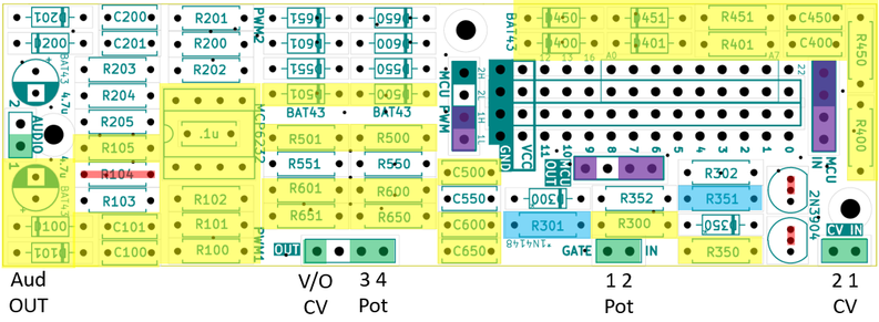
The following shows which components of the PCB will be populated (yellow), which will be changed for other components (blue), which wire links are required (red) and which connectors will be used for linking to the Pots and Jacks board (green) and MCU (purple).

Here is the list of components required for the above:

Resistors:

  • R100: 499K
  • R101, R102: 3.9K
  • R105: 200Ω
  • R300, R350, R400, R450, R600, R650: 1K
  • R401, R451: 100K
  • R500: 100Ω
  • R501: 330K

Capacitors

  • C100: 4.7nF
  • C101: 10nF
  • C102: 4.7uF electrolytic
  • R301, R351, C400, C450, C600, C650: 100pF (yes, two resistor slots are capacitors).
  • C400, C450, C500: 68nF

Other:

  • D100, D101, D400, D401, D450, D451, D500, D501: BAT43 Schottky Diodes
  • MCP6243

The mapping between IO connections and MCU IO pins is as follows (all other IO pins are not used):

MCU Connection PointMCU IO LinkFunctionMCU PWM 1H9Audio OUTMCU PWM 1L10Audio OUTMCU IN CV 2A7CV2MCU IN CV 1A6CV1MCU IN GATE 2A5Pot 2MCU IN GATE 1A4Pot 1MCU OUT 4A3Pot 4MCU OUT 3A2Pot 3MCU OUT 1A01V/Oct CV

Note: the order of the Gate/CV is (from top to bottom): CV 2, CV 1, G2, G1. The ordering of the OUT connections is the same for both sets of pin headers: 1 on the left, through to 4 on the right.

Build Order and Photos

This is the suggested build order:

  • Diodes.
  • Resistors.
  • Small capacitors.
  • Header sockets (assuming PH5 and PH3.5 sockets).
  • Capacitor on the rear of the board.
  • OpAmp.
  • Larger capacitors.
  • MCU board header sockets on rear of the board.
  • Jumper wires.

When installing R501, I’ve opted to make the fix described in the EuroRack 6HP MCU Experimenter Module Usage Notes and swap its position to the other side of R500 as shown below.

Otherwise the build proceeding pretty much as suggested.

Note that the OpAmp’s capacitor must be soldered to the rear of the board prior to fixing the OpAmp.

The install the OpAmp, smaller headers and larger capacitors.

Finally the longer headers for the MCU board can be installed on the rear of the board.

Finally the patch links can be installed as described previously (including the links instead of R104 and the transistors).

The Pots and Jacks Board

These functions will map onto the following potentiometers and jacks (and connections) from the EuroRack 6HP MCU Pots and Jacks PCB:

Pot/JackFunctionConnectionRV1Potentiometer 1GATE 1RV2Potentiometer 2GATE 2RV3Potentiometer 3OUT 3RV4Potentiometer 4OUT 4IN1V/Octave CV INOUT 1IN2CV 1 INCV 1IN3Not usedIN4Not usedOUT1Audio OUTPWM 1OUT2CV 2 INCV 2OUT3Not usedOUT4Not used

The pots and jacks PCB should be wired up to the interconnecting headers as follows:

Optionally, it might be useful to connect from the GND header pin to the panel once fitted.

It is suggested the Jacks and Pots PCB is built in the following order:

  • Small header pins on the underside of the board.
  • Long header pins (if used) on the underside of the board.
  • Jacks.
  • Potentiometers.
  • Link wires.

The Panel

This is the panel design required.

The measurements are all detailed in the EuroRack 6HP MCU Pots and Jacks PCB Build Guide, but crucially the pot holes are M7 and the jack holes are M6. I found they needed a 7.5mm and 6.5mm drill respectively to allow for a bit of flex when fitting the panel.

I’ve used M2 mounting posts, screws and nuts between the boards. In particularly, I found that the spacing required a 6mm spacer with an additional nut added as shown below.

I also had to break off the alignment lugs on the potentiometers to allow the panel to fit snugly.

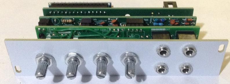
Once all together, you can see it needs around 45 to 50 mm clearance behind the panel for the whole thing.

Testing and Basic Code

I recommend performing the general tests described here: PCBs.

Then it can be connected to an Arduino Nano MCU board an a basic analogRead test can be performed to check the pots and input jacks.

void setup() {
Serial.begin(9600);
}

void loop() {
for (int i=0; i<8; i++) {
int aval = analogRead(A0+i);
Serial.print(aval);
Serial.print("\t");
}
Serial.print("\n");
delay(100);
}

An external potentiometer can be connected to a mono patch lead (GND and signal) and VCC to test the CV IN jacks (IN1, IN2, OUT2).

The order should be as follows:

A0IN 1 (1V/Oct)A1Not used, floatingA2POT 3A3POT 4A4POT 1A5POT 2A6IN 2 (CV1)A7OUT 2 (CV2)

The (dual) PWM output can be tested using the basic Mozzi “Hi-Fi” sinewave test which can be found in the examples here:

  • Examples -> Mozzi -> 01.Basics -> Sinewave_HIFI

Sample Applications

Here are other posts describing some sample applications for this module.

Closing Thoughts

I have to be honest – working out which parts of the circuits to use, then referring back to them to populate the PCBs, then soldering on the intra-board links and finally fiddling with the panel was actually quite a lot of work.

I don’t know if I’ve saved anything compared to just building the circuit from scratch on a piece of protoboard.

It is also going to be quite likely that any issues might be hard to trace too.

I might find that as I use more of these boards, (assuming I build some more of course), then I get to know the layout and circuits and won’t be referring back to the designs so much. I’ll have to see how it goes.

But for now, if all you want is a single Arduino Nano HAGIWO circuit, then you’re probably better off just making it up on protoboard…

But I think the whole board “sandwich” once complete does look pretty good!

I’ll have to see if I can get a bit of a “production line” going and make up a few more. And now I have to get on with some code…

Kevin

#arduinoNano #EuroRack #HAGIWO #mozzi

EuroRack 6HP MCU Experimenter Module

I’ve been following the work of HAGIWO for some time and always been really impressed with the breadth and range of modules they produce. I have noticed some patterns in their microcontroller…

Simple DIY Electronic Music Projects

EuroRack 6HP MCU Experimenter Module Usage Notes

Here are some suggestions and usage notes for my EuroRack 6HP MCU Experimenter PCB.

This post walks through the different sections of the schematic and PCB and shows how to tailor the circuits to different applications.

Here is a list of built modules using these boards:

Warning! These boards are meant for DIY systems only. They should NOT be used with expensive EuroRack modules, racks, or power supplies. I strongly recommend using old or second hand equipment for your experiments.  I am not responsible for any damage to expensive instruments!

If you are new to Electronics, see the Getting Started pages.

Introduction

As detailed in the design notes, there are a number of different sections for this PCB, each designed to be used to link a microcontroller to a EuroRack synth in a useful, and hopefully electrically useful way. There is also an additional PCB designed to support a range of configurations of Pots and Jacks for use with this MCU and IO board.

At various points, I refer back to a range of HAGIWO’s designs in the discussion (for a complete list see my design notes).

But I have to reiterate right at the start – I strongly state that you DO NOT use these in a rack of expensive or cherished gear!

It is meant for DIY experiments and so it should be expected that:

  • Use of this PCB could easily destroy any power supply powering it.
  • Use of this PCB could also easily destroy any EuroRack modules in the same rack using the same power bus.

In short, I’m only using this with cheap, second hand, other DIY kit, or equally sacrificial equipment and I strongly state that you should do the same.

The Microcontroller Board

Recall that there are two PCBs to be used: an IO board and a MCU board. The MCU board could support either a Raspberry Pi Pico (or similar) or an Arduino Nano (or similar).

The MCU board has all of the components on the underside, apart from the two rows of headers joining it to the IO board. The IO board has all components on the top-side, apart from the two rows of headers joining it to the MCU board.

Arduino Nano

The following illustrate which components are required to use an Arduino Nano. This shows the rear view of the MCU board.

The Arduino Nano will run directly off the EuroRack +12V line, so no regulator or associated components are required. The following detail shows which components need to be mounted to support the Nano’s power.

The Nano itself should be mounted on the two 15-way header sockets and aligned as shown below. Note that the USB connection is facing “down” towards the EuroRack power connector.

If the regulator and additional circuitry is already fitted it will be ignored if an Arduino Nano is used.

Raspberry Pi Pico

To use a Raspberry Pi Pico, the full power circuit is required, including the regulator, additional capacitors and diode as shown below. Once again this is showing the rear of the MCU board where all of the components (apart from the interconnecting headers) will be mounted.

The Pico will be mounted on the two 20-way header sockets and aligned as shown below, with the USB connector at the “top” facing away from the EuroRack power connector.

The IO Board

MCU Interface

The IO board itself will be connected to the microcontroller board using the interconnecting 14-way headers and all microcontroller IO pins will be broken out to pads as shown below.

The idea is that the main circuit sections terminate at one of the three MCU PWM|OUT|IN headers (also highlighted) and can then be patched across to the MCU IO headers which have the following layout.

GNDVCCD12D13(no)
D16A0A1A2A3
D17A4
D18A5
D19A6
D20A7
D21D22GNDVCCD11D10D9D8D7D6D5D4D3D2D1D0

The Arduino supports D0-D13 and A0-A7, although for an Arduino Nano A0-A6 can also be referenced as D14-D19 of course.

The Raspberry Pi Pico supports D0-D13, D16-D22 and A0-A2.

External Connections

Potentiometers, switches, jacks, audio or any other external IO can be connected to the IO board in a number of places. The following shows where they are and how they related to the MCU connections (assuming the appropriate circuitry in between has been connected up).

My additional Pots and Jacks PCB has been designed to match up with these headers and just needs a link to VCC and GND adding.

Which headers to use and how to do this is fully described in the Pots and Jacks PCB Build Guide.

Audio PWM Output

There are two PWM output channels, each of which can be driven by one or two PWM outputs from the microcontroller. A great explanation of dual PWM output can be found on Open Music Labs here:

PWM Resolution and Filter

The PCB will support a single PWM output by omitting R100. If dual PWM output is required, then R100 and R101 need to have values that support the required bit-depth of the PWM resolution as described in the Open Music Labs tutorial (see “table 2”).

Some options might be:

SourceR100R101Resistor RatioPWM ResolutionMozzi Dual499K3K9128Dual 7-bitProto Pedal PCB300K4K764Dual 6 bit

Otherwise a single resistor (e.g. R100) could be used for a single, 8-bit resolution PWM, in which case the chosen resistor will form part of the PWM filter consisting of R100 and C100.

As shown, there is a two-stage PWM filter circuit: R100/R101 and C100; R102 and C101. For a simpler application the second stage could be omitted and R102 replaced with a wire link (or short, for 0K).

In HAGIWO’s Nano design, the first stage uses values as per the Mozzi dual PWM default (above) with a 4n7 capacitor. The second stage uses a second 3K9 resistor with a 10nF capacitor. In the XIAO DAC application, HAGIWO uses a single resistor output from the DAC with a two stage filter of twin 10K + 1nF.

From the Open Music Labs tutorial, we have the following relationships for dual PWM and a low-pass filter:

  • R2 = R1 . 2^n
  • C ~= 1 / ( 2 . pi . R1 . Fc)

So the cutoff frequency Fc = 1 / ( 2 . pi . R1 . C ) where R1 is the smaller of the two resistors, so R101.

But when there are two filter stages, the RC calculation seems to be quite a bit more complicated and beyond my current knowledge of electronics, so I’m just going with some of the suggested values from the existing circuits…

Some options for the PWM filter stage I’ve seen so far can be summarised as follows:

R100R101R102C100C101Nano Dual7 bit499K3K93K94n710nNano Single8 bit–3K93K94n710nNano Single, Simple Filter8 bit–3K90K4n7–Nano Dual6 bit300K4K74K74n7 or 22n10nXIAO (3V3)8 bit DAC–10K10K10n10nRP2040 (3V3)10 bit (?)–220R220R10n10n“MOD1” design8 bit–1K0K1u–

Fundamentally, it depends on the required resolution, single or dual operation, and then the required cut-off frequency of the filter. For the simpler setup, values can be tested using a low-pass filter calculator (more here).

Note: I wasn’t able to easily source 499K resistors, but I was able to find a number of 500K 1% resistors so I used a meter to measure them and picked those closest to 499K.

Also note that the “MOD1” design has a very low cut-off frequency and is stated as being more for LFOs and EGs. More on that later.

OpAmp Gain

R103 and R104 can be used to set the gain of the MCP6232-based OpAmp. For 5V operation, R103 can be omitted and R104 shorted for unity gain. For 3V3 operation, the ration of R103 to R104 can be used to set a gain for 3V3 to 5V amplification. The values below were used by HAGIWO in the XIAO DAC output circuit.

R103R1045V to 5V (unity gain)–0K3V3 to 5V5K62K9

For a non-inverting OpAmp configuration, we have:

Vout / Vin = 1 + Rf / Ri

In this case we want Vout = 5 and Vin = 3.3 so Vout / Vin = 1.51; and we have Rf = 2K9 and Ri = 5K6 so Rf / Ri = 2900/5600 = 0.518.

OpAmp Choice

HAWIGO’s circuits often suggest the MCP6232 for rail-to-rail operation, but there are probably many others that would work too. There is a great OpAmp summary of Microchip offerings on their site that lists all of their OpAmps (see here).

I’m pulling out any dual, DIP packaged, rail-to-rail devices, that seem similar to the MCP6232 (I believe these all have the same pinout):

DeviceGBWPIQ TypVOS MaxOp VoltageMCP6232300 kHz20 uA7 mV1.8V to 5.5VMCP6242650 kHz50 uA7 mV1.8V to 5.5VMCP60021 MHz140 uA4.5 mV1.8V to 5.5VMCP62722 MHz170 uA3 mV2.0V to 5.5VMCP62752 MHz150 uA3 mV2.0V to 5.5VMCP62825 MHz445 uA3 mV2.2V to 5.5VMCP62855 MHz400 uA3 mV2.2V to 5.5VMCP629210 MHz1000 uA3 mV2.4V to 5.5VMCP629510 MHz1100 uA3 mV2.4V to 5.5V

Of course, I’m quoting those figures with very little clue as to their meaning, but in my “hand-wavy” world of electronics knowledge, given the kind of level I’m working at here, I would suggest any of those might be fine for this application.

Most are probably rated more highly than required, and I’d suggest the lower current ones are best for the audio frequencies I want to be working at.

I’ve also seen at least one circuit suggesting the NJM2732, which appears to be another rail-to-rail OpAmp with an operating voltage of 1.8 to 6.0V and GBWP of 1MHz, so I’m going with the idea that again for my Lo-Fi world, that is essentially interchangeable with the above.

One other thing to note. These are all dual OpAmps, but if only one is used, then it isn’t obvious what to do with the spare pins of the other.

It would appear that the best solution, assuming using a single OpAmp variant isn’t an option, for a single supply configuration, is to feedback from the output to one of the inputs and connect the other to a reference voltage as follows:

This is taken from the Texas Instruments TechNote “How to Properly Configure Unused Operational Amplifiers”.

Having said that, this other TI blog also notes that it probably isn’t the end of the world if this isn’t done: “most modern op amps have independent biasing circuitry, unperturbed by overloads in other channels on the same chip. If your circuits are working, relax and follow best practices in your next design.”

Interestingly, the MCP6231/1R/1U/2/4 datasheet section 4.5 “Unused Op Amps” seems to imply this only applies to the quad MCP6234…

Output Coupling

The final stage of the circuit sets the output impedance and removes the DC bias from the audio output. I’ve seen all of the following values used so far:

R105C102XIAO DAC Output470R2u2Nano Output220R4u7RP2040330R10u

I’ve not spent any time wondering about how these values will affect the output, so I’m just documenting them for now. This is probably a good area for experimentation to find the most suitable values for any specific application.

The two diodes (D100, D101) that provide clamping are BAT43 Schottky diodes.

Second PWM Output

All of the above can be duplicated for R200-205, C200-202, D200-201 for the second PWM channel, which uses the second OpAmp from the MCP6232.

In the photo below, all components and connections associated with PWM 1 are highlighted in RED and for PWM 2 are highlighted in YELLOW. naturally if only one PWM circuit is required, all components associated with the other can be omitted.

GATE and CV Inputs

There are two GATE and two CV inputs as shown in the following schematic sections – GATE input on the left; CV input on the right.

Gate Input

The GATE input section mirrors that of my Educational DIY Synth Thing, so the values are pretty much fine as being the following:

R300100KR3011MR30210KD3001N4148

Note that the actual MCU_GATE_IN signal will be active LOW – so inverted compared to the input signal. The input signal is assumed to be a 0 to 5V signal.

R302 is just a pull-up resistor, and everything should be fine with either a 5V or 3V3 VCC level.

CV Input

The CV input section has several variants. R400 and R401 can be used as a potential divider if the input voltage needs adjusting. Some examples of the components used are as follows:

R400R401C400Common 1V/Oct1K100K68nNano 1V/Oct100R100K68n5V CV to 3V3220K330K10n5V CV to 3V322K33K10n“MOD1” design1K100K10n

Note that in most cases D400 and D401 are BAT43 Schottky diodes (in the “MOD1” design, 1N5819WS were chosen).

When the ratio of R400 to R401 is close to 1, then essentially almost the whole voltage range, up to the clamped voltage rails, is used as input.

When the ratio of R400 to R401 is ~2/3 then the output voltage will be approx 3V3 (max) from a 5V input. There are two values that seem to be used: 22K to 33K or 220K to 330K.

I’ve since seen a note that R401 should really be between the external connection and R400 for 5V systems, which would remove the potential divider effect. This is shown below.

Whilst the board doesn’t directly support this, it is possible to patch that in as shown below.

Note: any of the blue spots are GND connections and could be used. In fact, looking at the traces, it would be possible to swap R451 and C450 over, and the same for R401 and C400 – this would leave some spare GND pads where the capacitors were originally placed that could then be easily used for the moved resistors.

Whether this is actually required or not is left as an exercise for the reader – in other words, I’ll get back to it after some experimenting! The “MOD1” design doesn’t worry about this for example.

Potentiometer Input

If a slightly more robust potentiometer input is required, then it is possible to use the CV input circuit without the clamp diodes and omitting R401 as follows:

In this case it would be recommended that R400 = 1K. HAGIWO suggests C400 = 100pF, but I’ve used 10nF for potentiometer smoothing before. Naturally a pot could just be wired directly to the microcontrollers analog inputs of course.

The “MOD1” design uses R400 = 10K and C400 = 10nF with a 100K pot.

Second GATE and CV Input

Components R300-R302, D300 are repeated as R350-R352, D350 to give a second GATE input. Components R400, R401, C400, D400, D401 are repeated as R450, R451, C450, D450, D451 to give a second CV input. The relevant areas are shown below.

  • Gate 1 – Yellow
  • Gate 2 – Red
  • CV 1 – Purple
  • CV 2 – Blue

Once again, any unused sections can be omitted completely.

Additional Potentiometer Inputs

It is also possible to use the GATE stage as a potentiometer input too as shown below.

In this case, pull-up resistor R302, diode D300, and the transistor are omitted, but pins 2 and 3 (the two oval pads, left and centre) of the transistor need connecting. then R301 is replaced with a capacitor and the output of R300 connected to the potentiometer “wiper” via the GATE IN link.

Aside: it is also possible to repurpose an OUTPUT stage for a potentiometer INPUT too by omitting the clamp diodes and one of the resistors, as shown below:

But of course, in this case MCU_OUT_1 becomes an MCU_IN connection – a little confusion, but definitely possible. More on the OUTPUT circuits in a moment.

Additional CV Inputs

Whilst on the topic of changing uses, it is also possible to repurpose a GATE input as a CV input as follows.

In this case, R302 and D300 are both replaced with BAT43 clamp diodes and the transistor is omitted, with pins 2 and 3 connected together. To complete the CV in circuit as shown previously a capacitor could also be soldered to the same connections as R301.

GATE and CV OUTPUTS

There are four generic OUTPUT circuits which could be used for either GATE or (PWM generated) CV signals.

The key difference being that for a GATE OUTPUT, R501 and C500 can be omitted. D500 and D501 are BAT43 Schottky diodes once more. Some sample values and applications are shown below.

R500R501C500GATE OUTPUT470––CV OUTPUT470–4u7“MOD1” design1K100K or omitted1uF

R501 is not really needed in the above. Truth be told, I can’t remember why I thought I ought to include it! It is there in the “MOD1” design, but it isn’t clear to me why.

It does however leave the possibility that these nominally output circuits could be repurposed as additional inputs if required (this might be why they feature in the “MOD1” design). With all the components fitted, it is essentially mirroring the CV input circuit discussed previously.

Note that for CV generation from PWM, those stated C500 and R500 values give quite a low cut-off frequency:

  • 470R + 4u7 ~ 70Hz
  • 1K + 1uF ~ 160Hz

These could be adjusted, but I guess the main idea is that these are slower changing control voltages such as from an LFO or envelope generator rather than an oscillator out, which ought to the use more complete PWM “audio” output stage previous mentioned.

Four Output Stages

Each output stage is independent, and the relevant components are shown below. Once again, any unused sections can be omitted.

Key:

  • Output 1 – Yellow
  • Output 2 – Red
  • Output 3 – Purple
  • Output 4 – Blue

Closing Thoughts

This was never intended to be a completed board, it was always meant to make it easy to experiment with different options. The downside of that approach of course is that none of the circuits have really been tested yet at all, so it is all theory at this point.

Having seen with hindsight how various sub circuits can be repurposed, it would have been nice to design those options in more officially – via jumpers or silkscreen updates for example. But as the board is pretty packed already, I suspect my options here would be quite limited.

Either way, I think it should support my experiments pretty well so am pretty pleased with how it turned out.

Kevin

#arduinoNano #EuroRack #pcb #raspberryPiPico

EuroRack 6HP MCU Experimenter Module PCB Build Guide

Here are the build notes for my EuroRack 6HP MCU Experimenter Module.

Warning! I strongly recommend using old or second hand equipment for your experiments.  I am not responsible for any damage to expensive instruments!

If you are new to Electronics, see the Getting Started pages.

Bill of Materials

  • EuroRack Control IO PCB (GitHub link below).
  • EuroRack Control MCU PCB (GitHub link below).
  • EuroRack 6HP Panel PCB (GitHub link below).
  • Arduino Nano or Raspberry Pi Pico.
  • Either 2x 15 way headers (Nano) or 2x 20 way headers (Pico) – PH5 headers recommended.
  • 2x 14-way header pins and socket – PH5/9.5mm headers recommended (see below).
  • Header pins.
  • 1x 1N5817 Schottky Diode.
  • 1x 10Ω resistor.
  • 1x 47uF electrolytic capacitor.
  • 1x 2×8 way shrouded pin header socket (EuroRack power).
  • M2 mounting posts, screws, nuts as required.
  • Jumper/connecting wires.

Power supply circuit (Pico only):

  • L7805 regulator.
  • 1x 1N5817 Schottky Diode.
  • 1x 47uF electrolytic capacitor.
  • 1x 100nF ceramic capacitor.

Note the above are the minimal set of components required before actually building in specific circuits.

A note on headers. I’m using “PH5 short profile” headers which don’t stick out as much as normal headers. I’m matching these with 9.5mm long header pins. The difference can hopefully be seen below.

Note: there are “PH3.5” headers too, which need 7.5mm long pins, but I’ve stuck with the PH5.

Some typical components required for the actual circuit modules are as follows. The quantity and values will vary according to the actual circuit built of course.

  • BAT43 Schottky diodes.
  • MCP6232 OpAmp and (optional) 8-pin DIP socket (for PWM audio output).
  • 2N3904 NPN general purpose transistors (for Gate/Trigger IN).
  • Resistors – various.
  • Ceramic capacitors – various.
  • Electrolytic capacitors – various.
  • Potentiometers, jacks, switches, etc. – as required.

Build Steps

Taking a typical “low to high” soldering approach, this is the suggested order of assembly for the MCU board:

  • Resistor and diode(s).
  • Regulator (if used).
  • Capacitors.
  • Microcontroller headers.
  • Eurorack power header.
  • PCB connecting headers.

The order of assembly for the IO board will depend on the components and circuit being built, but it is recommended that the connecting headers are soldered on before any connections are made from the rest of the board to the header.

This is the general suggested order of assembly for the IO board.

  • All diodes.
  • All resistors.
  • DIP socket.
    • Note: one of the capacitors has to be fitted within the footprint of the DIP socket. This is probably easier to do on the rear of the board and possibly prior to fixing the DIP socket.
  • Disc capacitors.
  • Transistors or regulator.
  • Pin headers.
  • Electrolytic capacitors.
  • PCB connecting headers.
  • Inter-circuit connecting links (if not using headers).

Be sure to check the components are being soldered to the correct side of the boards. Most of the components (apart from the connecting headers) for the MCU board are on the rear. Most of the components (apart from the connecting headers) for the IO board are on the top side.

Any controls (potentiometers, switches, jacks, and so on) will have to be fixed to the header connections on the IO PCB. It is possible to use header pins and jumper wires, but a better result will probably result from using directly soldered connections. YMMV…

If using my EuroRack panels, then there are GND and VCC rails that can be used to make adding IO controls easier, but these will need to be connected to the power rails of the IO PCB at some point too.

Here are some build photos for the Raspberry Pi MCU board.

Here are some build photos for the Arduino Nano board.

Here is the build photo for the IO board.

Generally, although it might be a little tricky to solder around the header, it is still advisable to solder the headers on before making the final intra-board links.

This is because it is highly likely that some of the patch cables will need to pass over the solder-side of the headers.

Alternatively it might be possible to make the intra-pcb links on the underside of the board, meaning all soldering can be performed “from the top”. In this case, it might be advisable to put the headers on first…

Testing

I recommend performing the general tests described here: PCBs.

It is strongly recommended that all unused EuroRack power connections are checked and verified that they are unconnected to each other, +12V and GND.

Then it is really down to checking the power supply is working and all of the MCU IO is correctly present on the IO board once both boards are connected.

It is strongly recommended that the board is tested on its own, completely independently of any other modules or an expensive EuroRack power supply. In fact, it is NOT recommended that these boards are used with any other modules or an expensive EuroRack power supply at all. They are designed for use with cheap, DIY systems only.

PCB Errata

There are the following issues with this PCB:

  •  Nothing at present.

Enhancements:

  • With hindsight, I’ve have probably added some GND/VCC connections on the IO board around the edge to make wiring up to panels and controls a bit easier.
  • I could probably switch the position of the central mounting hole and shuffle some of C500, C550, C600, or C650 which would then probably allow for a companion mounting hole on the MCU board, where this is currently some spare space on the PCB.
  • I thought to add some headers for power on the MCU board, but it might have been useful to include two headers – one on each side of the board – to allow simple jumpering across from one board to another, to save on the cabling requirements of every board being connected back into a EuroRack system and to pass on the 5V connection if required.
  • I should have some panels produced with mounting holes in the right place to fit these PCBs directly.
  • Alternatively a third PCB could be produced with mounting headers to connect to the audio, INPUT and OUTPUT headers of the IO board to support the mounting of pots, jacks and switches.

Find the IO and MCU PCBs on GitHub here.

Find the blank panel designs on GitHub here.

There are also some templates which can be used alongside the Usage Notes to document and design new circuits in the GitHub too.

Closing Thoughts

My boards power up. There is 12V and 5V largely where I expect it to be and both variants seem to power up their respective microcontrollers ok.

Kevin

#arduinoNano #EuroRack #pcb #raspberryPiPico

EuroRack 6HP MCU Experimenter Module

I’ve been following the work of HAGIWO for some time and always been really impressed with the breadth and range of modules they produce. I have noticed some patterns in their microcontroller…

Simple DIY Electronic Music Projects