Quantum dot qubit using High NA EUV lithography | imec

The most advanced lithography system, crucial for future advanced memory and computer chips, will play a key role in scaling up quantum technology.

imec

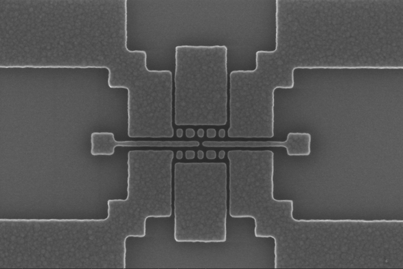
imec presented a silicon quantum dot spin qubit, which confines an electron within a silicon nanostructure, built with ASML High-NA lithography equipment.

This is a meaningful development because unlike some other qubit technologies this architecture can be produced with high-throughput commercial equipment.

https://www.imec-int.com/en/press/world-first-imec-presents-quantum-dot-qubit-device-using-high-na-euv-lithography

#HighNA #EUV #Lithography #QuantumComputing

Quantum dot qubit using High NA EUV lithography | imec

The most advanced lithography system, crucial for future advanced memory and computer chips, will play a key role in scaling up quantum technology.

imec
📢 Behold! #Imec has managed to conjure up some 20nm metal lines using EUV wizardry, which is clearly only for the chosen ones who understand what "High NA" even means. 🔍✨ Meanwhile, we mortals are still trying to figure out if "imecExpertise" is a legit word or just a desperate attempt to sound smart. 😂🔬
https://www.imec-int.com/en/press/imec-demonstrates-electrical-yield-20nm-pitch-metal-lines-obtained-high-na-euv-single #EUVtechnology #semiconductor #HighNA #innovation #HackerNews #ngated
Imec demonstrates electrical yield for 20nm pitch metal lines obtained with High NA EUV single patterning | imec

First electrical tests at 20nm pitch present a next milestone in validating the High NA extreme ultraviolet (EUV) patterning ecosystem

imec
https://youtube.com/watch?v=h_zgURwr6nA&si=MCQgzbSUXuscSmmp #asml #highna #euv en daar mag ik dan een klein deel aan bijdragen
Unveiling High NA EUV | ASML

YouTube
#TSMC’s CEO Visited #ASML Headquarters In Secret, Heralding A Possible Change In The Company’s Approach Toward #HighNA #EUV #Lithography
TSMC's arch nemesis of sorts, #Intel, has staked its very survival on achieving an insurmountable lead in the emerging field of High-NA EUV lithography. In fact, the first few such machines are all destined for Intel's chip fabrication units.TSMC said they would not economic sense before 2026, may be rethinking that clear-cut stance.
https://wccftech.com/the-secretive-visit-of-tsmc-ceo-to-asml-headquarters/
TSMC’s CEO Visited ASML Headquarters In Secret, Heralding A Possible Change In The Company’s…

TSMC has previously stated that its current lineup of Low-NA EUV lithography machines can support production well into 2026.

Wccftech
#ASML sets new #EUV chipmaking density record, proposes #HyperNA tools and radical EUV speed boosts
SML’s standard #LowNA EUV machines can print critical dimensions of 13.5nm, and the new #HighNA #EXE5200 EUV tool is designed to create even smaller transistors by printing #8nm features.
They also outlined a plan to reduce EUV chipmaking costs by radically boosting the speed of future ASML tools to 400 to 500 wafers per hour, more than double the current peak of 200 wph.
https://www.tomshardware.com/pc-components/cpus/asml-sets-new-chipmaking-density-record-proposes-hyper-na-tools-and-radical-euv-speed-boosts
ASML sets new EUV chipmaking density record, proposes Hyper-NA tools and radical EUV speed boosts

Smaller, faster transistors at unprecedented speed.

Tom's Hardware

إنتل تُكمل تجميع أولى أجهزة طباعة الرقاقات High-NA EUV في العالم

https://todaypic.net/technology/168439/

إنتل تُكمل تجميع أولى أجهزة طباعة الرقاقات High-NA EUV في العالم

إنتل تُكمل تجميع أولى أجهزة طباعة الرقاقات High-NA EUV في العالم حصلت شركة إنتل في الآونة الأخيرة على اهتمام وسائل الإعلام لكونها أول صانع لأشباه الموصلات يستخدم أجهزة طباعة الرقاقات High-NA EUV عا…

TodayPic
#Intel is buying leading-edge #lithography tools — Intel will acquire 6 of 10 #highNA #EUV tools from #ASML next year. Used for production of chips using Intel's #18A technologies in 2025. Intel will likely be first company to initiate high-volume production with high-NA tools, and will set industry standards, which will probably give Intel strategic advantages over rivals from #TSMC and #Samsung which has also reached an agreement to obtain high-NA EUV tools from ASML
https://www.tomshardware.com/pc-components/cpus/intel-is-buying-leading-edge-lithography-tools-report-says-intel-will-acquire-six-of-10-high-na-euv-tools-produced-by-asml-next-year
Intel is buying leading-edge lithography tools — report says Intel will acquire six of 10 High-NA EUV tools produced by ASML next year

Samsung has also reached an agreement to obtain high-NA EUV tools from ASML

Tom's Hardware
#NewYork set to host $10B #semiconductor research facility with #IBM and #Micron
Planned facility to include advanced chip-making equipment made by #ASML the sole global supplier of extreme #ultraviolet lithography (#EUV) machines capable of defining #silicon features at the smallest scale. Tipped to be one of the first recipients of machines featuring ASML's high numerical aperture (#HighNA) technology, for #2nm chips https://www.wsj.com/tech/new-york-joins-ibm-micron-in-10-billion-chip-research-complex-475437b3
WSJ News Exclusive | New York Joins IBM, Micron in $10 Billion Chip Research Complex

Planned facility to include advanced chip-making equipment made by ASML

WSJ
#HighNA will be critical in facilitating the production of advanced semis needed for #AI, #5G and high-performance computing at an acceptable cost, thereby helping to drive the global semis market towards a ca. $1trn level by 2030, notes @GoldmanSachs