Hello and welcome to the #nakeddiefriday again. This one will be a continuation of the previous one with the same exhibit but in more depth. :-)

To remind you, this is the unnamed smartcard IC, which I believe was fabbed by Samsung.

Let's try removing some metal from the top. ๐Ÿงต

#electronics #reverseengineering #smartcard

Interestingly, the thick infill area was way more resistant to the lapping process and the majority of metal-3 remained there, while the rest got stripped off.

There is a lot of analog circuitry on the bottom and right sides of the chip. I am not sure why there is so much and what it does exactly.

A detail view on the analog section; the features on the right seem to be four resistor arrays of the same value, and those on the left are multiple capacitors connected in parallel. I wonder why they decided to make multiple separate parts instead of making a large one of required geometry.
A detail view of the sea of gates. Note the difference in the shade of blue.
The smaller memory array in bottom left is certainly an SRAM block.
Then the array in the middle is actually the mask ROM. That's a lot of code space. Bit density is impressive as well, looks like an implant NAND ROM. 10 poly lines going horizontally, 8 routed from the vertical metal-1 and two from the circuitry in the center, likely enable lines. Looks like a very typical architecture for such memory.
Part of the EEPROM circuitry, looking almost-symmetric.
Finally there is this zone, which I also noted last week. I can't say for sure, but this does look like a PLA.
And there is this pad circuitry. This pad was not bonded out. I am intrigues by the unusual square feature in the upper left quadrant.
Removing most of metal-2, we get a better view on the circuitry. Unfortunately, I am not skilled enough yet to correct the material removal location, so it turns out uneven.
The SRAM now very clearly displays the bit cell structure. Each of the suiggle pairs is in fact two inverters connected in a loop.
The more-or-less same portion of the mask ROM for comparison. Clearly, metal-1 is primarily used for local routing.
This is displayed even more clearly in the sea of gates. Removing metal-2 makes each individual gate stand out. In several cases metal-1 is used for global routing here.
There has been an interesting development in the "PLA" area too. Now a pattern can be seen on the right here. This looks almost like a binary counter.
Looking at the funky pad again, now I can see what this is about. It is a fuse. And it looks not to be blown, which is rather interesting.
The same analog component blocks as before, indeed a set of individual resistors and capacitors.

Finally, there is something that can be classified as human-readable text. I fail to extract any meaning from this.

EDIT: People smarter than myself suggest this may have been LOW_TEMP.

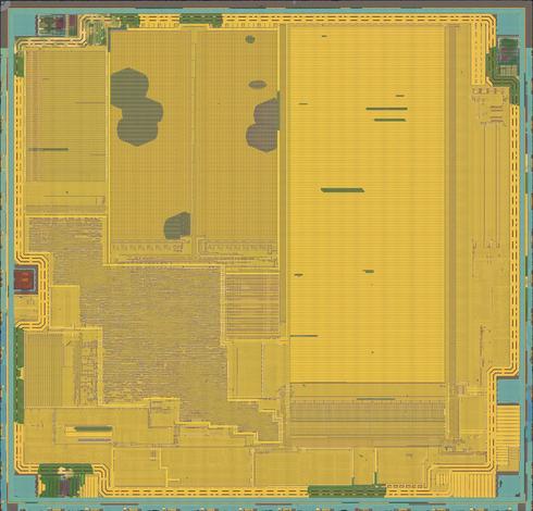
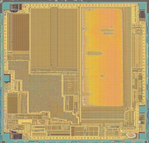
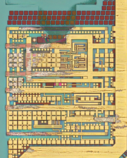
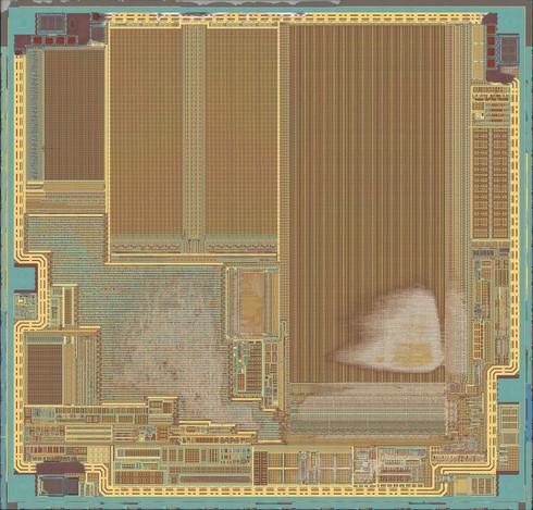
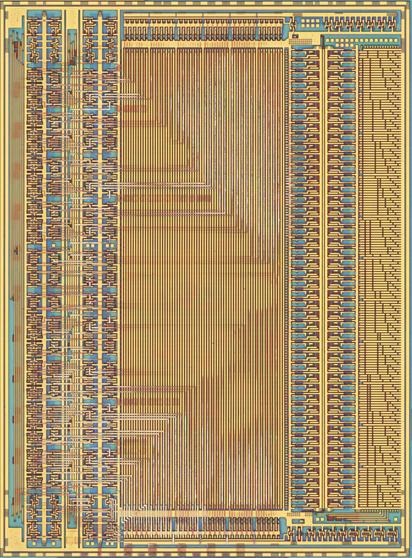
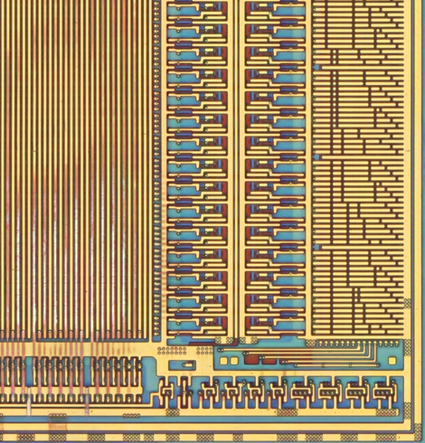
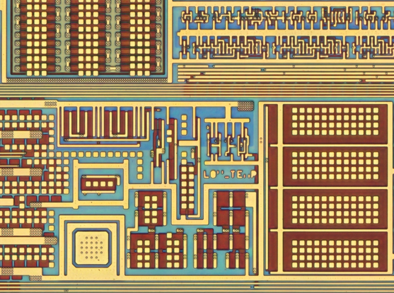
Aaand there is no next deprocessing step, because I managed to lose this sample too while trying to get metal-1 off. Thus, the thread ends here. This made me very sad, and pointed to an obvious area needing improvement in my process.

I hope you enjoyed looking at the construction of a more complex chip in detail as much as I did taking these images. As always, I will appreciate any and all support to offset the costs of consumables required to do this work.

I wish you all a great end of this week. Stay safe, stay healthy, and I hope to see you all next Friday.

@infosecdj Do you suppose it was once "LOW_TEMP" but a design rule checker deleted the diagonal-ish parts of the W and M?
@acsawdey A great guess! This could very well be the case, although I wonder why such a text might be there... Could this be a temperature sensor?
@infosecdj @acsawdey Someone put it on the wrong layer?
@acsawdey @infosecdj independently had the same thought!
@infosecdj god its so pretty
@0x00string I only wish I had more samples of this chip :)
@infosecdj yours is one of the best accounts on here.
@0x00string Thank you! I appreciate your kind words.
@infosecdj What node is this? You're getting beautifully sharp optical images indicating it's nowhere near at the limits of optical resolution, yet it's also multiple metal layers, standard cell based, planarized, etc. That's not a combo I see too often.
@azonenberg If only I knew. This certainly seems to be on the larger side, as everything is very well resolved indeed, at least on metal layers. Poly might get close to the limits of at least my system, the ROM is challenging to resolve well.
@infosecdj it feels like 350 give or take a node
@azonenberg I measured the metal-1 wire width, which came in about 677nm. Poly wiring looks about the same width. Again, a large margin of error as it is only about 13 pixels wide and the setup is not perfectly calibrated.

@infosecdj So could be a 500ish nm class node then. That would make sense, I've seen one 500nm node (on the FT232R) that was planarized.

Usually once you go much larger it's non-planar though

@infosecdj oh boy, just the sea to make a puzzle of!
@infosecdj for example on a bit bigger scale :)