Starting to dust off the Ethernet switch project and make some strides towards finishing it.
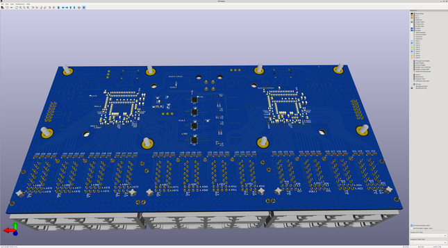
First step: preparing to populate the back side of the remaining switch line cards. I hand assembled one a year or so ago and then the project got put on ice while I got busy with higher priority stuff.
But now that my friends are starting to get their PnP operational, I'm gonna try and run the rest of the boards on it.
Just inventoried components for the back-side assembly run and ordered a reel of 0402 zero-ohms because I seem to have misplaced my current one (all I have are the loose ones in a pill organizer from when I was starting out, I swear I had a few hundred on cut tape but they're not where they should be).
I ordered five PCBs originally and populated one by hand, so I have four left over. The plan is to populate three fully since I need a total of four (two 24-port line cards per 48 port switch, two switches).
And since the marginal cost of populating an extra board on the PnP is pretty low, I'm gonna stuff one more but leave all the expensive connectors and semiconductors off. I want to do some 2-port shunt-through VNA measurements on the PDN and get some real world impedance measurements. Not that it's necessary, the design is already brought up and working, but it'll be a good test and validation for the future.