Guide to the TD4 4-bit DIY CPU
https://www.philipzucker.com/td4-4bit-cpu/
#HackerNews #DIYCPU #TD4 #4bit #Technology #Hardware #HackerNews
Guide to the TD4 4-bit DIY CPU
https://www.philipzucker.com/td4-4bit-cpu/
#HackerNews #DIYCPU #TD4 #4bit #Technology #Hardware #HackerNews

@niconiconi This looked like such a great publication, at one point I was seriously looking to see if I could get a copy, after messing around quite a lot with the #TD4 CPU design myself. But ultimately had to decide there would be little point giving my lack of language skills.
But I was still looking if I could get copy. I mean, this really is such a great publication! :)
I appear to have created a "sound card" for a 4-bit CPU.
As you do.
TD4 4-bit Sound
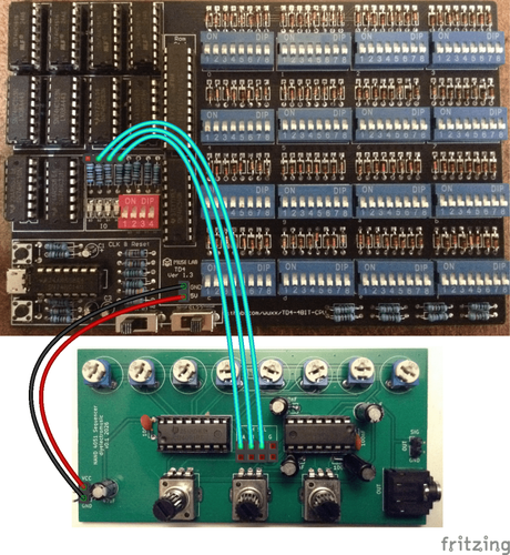
Over on my other blog, I spentt a fair bit of time looking at the TD4 4-bit CPU. One of the things I wanted to do with my NAND Oscillators and Logic Sequencer PCB was hook up the address/select pins to something else. And with three select pins, allowing the choice between 8 notes, what better to connect it to, than a 4-bit CPU?
https://makertube.net/w/aroDZYM2BHYpoB9QLJvHnk
Warning! I strongly recommend using old or second hand equipment for your experiments. I am not responsible for any damage to expensive instruments!
If you are new to microcontrollers, see the Getting Started pages.
Parts list
The Setup
The most obvious thing in my mind, is to hook up three of the four outputs to the three selection pins of the NAND sequencer, so that is what this post explores.
The NAND PCB needs the jumpers removing, which disconnects the pot-driven oscillators. Then the three select/address lines can be connected to three of the four resistors supporting the OUTPUT LEDs of the TD4, as shown above.
It is also possible to use the POWER header pins to power the NAND PCB too.
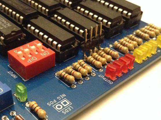
Any of the variants of TD4 I’ve built could be used, but I’ve shown above where they would need to be connected on the original. In the end I actually soldered four header pins to the appropriate side of the resistors on my own PCB version of the TD4 as shown below. A bit crude, but it does the job.
Connecting these over to the NAND sequencer and hooking up power gives me the following.
The Code
The simplest way to create a sequence is a set of OUT xx instructions where the least significant 3 bits (so values 0 to 7) map onto the three possible notes played by the NAND sequencer.
This is the simple LED OUTPUT code from Part 3 of my series, but this continually toggles between the lowest and highest notes.
0000 OUT 0001 # 1000 1101A counter can be used to play all 8 notes. Note that in this code B will go from 0 to 15 (b0000 to b1111) but only the last three bits select notes. This means that the sequence will count from b000 to b111 twice for each pass through this loop with the top bit being ignored.
0000 ADD B,0001 # 1000 1010There are only two speeds though, 1Hz and 10Hz so the above, which has three instructions, has a tempo of 20 bpm (1 note every 3 seconds) or 200 bpm (approx 3 notes every second). The tempo can be slowed down in steps of 1 second or 1/10 second by moving the JMP an instruction further down and back-filling with other instructions (ADD A,0 or b00000000 is a good one, and is essentially equivalent to a NOP).
The following code uses the INPUT as a counter in a loop to provide a partly configurable tempo.
0000 IN A # 0000 0100 A = INPUTThis is still only cycling through each note individually though, but that is kind of what an 8-step sequencer would do.
To get more creative with the programmability of the sequencer requires a series of OUT instructions and NOPs between them, for example:
0000 OUT 0000 # 0000 1101 OUTPUT = 0000 # Play note 000This last programme is the one running in the video at the start of this post.
Closing Thoughts
I appear to have made a sound card for a 4-bit CPU 🙂
One thing I am quite keen to do is connect up the sequencer’s select pins to the TD4’s address lines, as I’d like to be able to have some incidental (accidental?) music that appears as a result of the CPU just running any other normal programme.
To do this I’d need to either hook into the output of the PC register or the input to the HC154 ROM decoder.
In fact, it would be really interesting to be able to hook up any sets of four signals – so the INPUT selector, or even the control decoding logic – just to see what it sounds like as the CPU is running normal code. That might require a special build of the CPU though.
I also have an address line spare of course, so it would also be interesting to use that to select between two NAND sequencers to give me a 16 step sequence.
Kevin
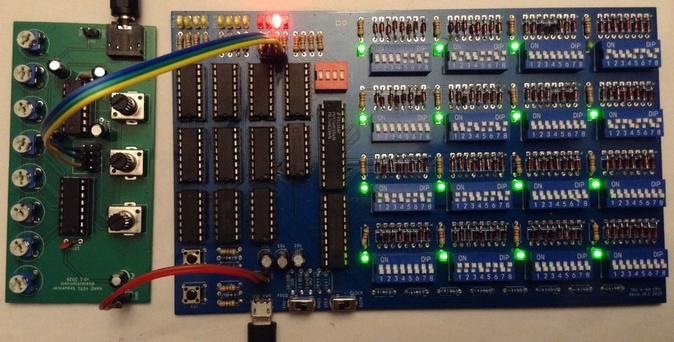
TD4 Sequencer and NAND Oscillators

The PCBs work! Here it is in action. Now with extra bling! :)

TD4 4-bit DIY CPU with Arduino Nano ROM
And here is the accompanying blog post describing the theory and design.
https://emalliab.wordpress.com/2025/11/26/td4-4-bit-diy-cpu-part-8/
TD4 4-bit DIY CPU – Part 8
Now that I’ve shown I could support more ROM if required using a microcontroller (see Part 6) I can start to ponder how that might be possible.
There are several other expansions to consider too. Other things I’m pondering are:
And probably a few other odds and ends as I go back and reconsider the schematic as it stands, but they can wait for a future post.
TD4 Simulation
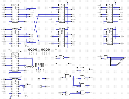
Before I get stuck into the updates, I thought it would be useful to be able to simulate the TD4 to allow for quick turn-around experiments.
I’ve used the “Digital” logic simulator which can be found here: https://github.com/hneemann/Digital
I could have build the simulator from basic logic gates and that would perhaps have been more useful in helping to understand how the design works. But I wanted something that would be easy to fiddle about with to test enhancements, so I build it using the actual 74xx logic chips instead. This doesn’t make for such a readable simulation, as I’ve had to go with actual pinouts for chips rather than logical groupings of signals. But it does map more closely onto the final hardware which is handy for thinking in actual chip-usage rather than abstract logic.
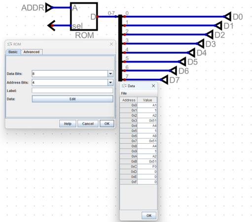
I’ve not bothered simulating the clock circuit, I’ve just wired in a clock source. I’ve also not added the ROM DIP switches, instead adding a ROM element and wiring it into the address and data lines. By right-clicking and viewing the attributes, it is possible to define a 16-byte ROM (4 address, 8 data lines) and edit the contents.
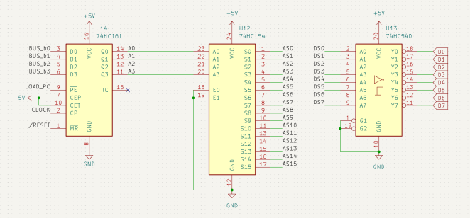
The ROM element takes a multiplexed source and produces a multiplexed output, so I use a splitter/mixer function to turn that into D0-D7 as shown above. Similarly the output of the 74HC161 acting as the program counter (PC) has A0-A3 mixed into a single ADDR bus line.
I’ve added outputs to the two registers to show their contents during execution. I’ve also added a DIP switch on the /RESET line to allow me to start and stop the simulation.
The video below shows it running the above ROM contents, which is the same demo program I used in Part 6 with the microcontroller ROM.
The simulator can be found on GitHub here: https://github.com/diyelectromusic/TD4-CPU
https://makertube.net/w/5njzGmYvqXiU3DLCMMtwqp
Now I have an easier way of experimenting, onto the enhancements.
Increasing the Address Space
The address space is currently implemented as follows:
The counter auto increments on each clock pulse, thus moving through the address space, but it can also be a destination for the adder, allowing absolute jumps to specific addresses, thus implementing a JMP instruction.
To increase the address space, there are a few considerations:
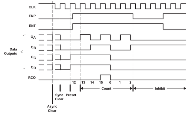
One idea is to use the RCO pin of the 161. This is the “ripple carry out” and can be used to cascade counters for greater than 4-bit counting. As I understand things, RCO will be HIGH once all outputs are also HIGH, for a single clock pulse. This can be used to enable a following counter for that pulse. This is shown below (taken from the datasheet).
And this is the sample application, again from the datasheet, showing how it would work, with extensions on to additional stages.
A simple way to add an additional bit of address space might be to feed RCO into a flip-flop acting as a toggle in the configuration shown below.
This can then be used to select between two HC154 4 to 16 decoders. As I already have an unused flip flop as part of the HC74 used for the CARRY, this could be quite an appealing solution and in simulation it does appear to work.
There is one slight complication. As show above, A5 will toggle with A0-A3 = 1111 not as they change back to 0000. This is because the flip-flop toggles on the rising edge of the provided clock signal, which in this case is RCO from the 74HC161. Adding a NOT gate means that the rising edge happens as the 161’s RCO signal drops when it resets back to 0000.
Whilst this solves the sequencing problem it does have the unfortunately side effect that the RESET state means that A5 is 1 on power up. That too could be solved with another NOT gate if required, or simply hanging A5 off the /Q output of the flip-flop rather than the Q output.
Here is the additional wiring, in simulator form, to allow this to work.
Note the addition of A4 which now comes from the spare flip-flop /1Q output, and the linking of RCO via a NOT gate to the flip-flop 1CP clock input. The rest of flip-flop 1 is configured in toggle mode, with /1RD and /1SD both tied high (inactive) and 1D linked to /1Q for the feedback. The non-inverting output 1Q is not used.
Whilst this seems to require an additional logic gate (for the NOT) it turns out that there is a spare Schmidt trigger inverter on the 74HC14 that supports the clock circuit, so that is pretty convenient.
The ROM has also been reconfigured for 5 address inputs with the same 8 data bits, creating a 32 x 8 bit ROM.
There are a few issues with this though:
But if one can program around those constraints this is quite a simple solution.
An Alternative Solution
There is a neat solution to adding a 5th address bit here: https://xyama.sakura.ne.jp/hp/4bitCPU_TD4.html#memory
This uses the duplicate JMP/JNC instructions to encode a JMP2/JNC2 that results in the 5th address bit being set, this enabling a jump to the second half of the memory.
In order to create the additional address line, there is a second PC register added – i.e. a 5th HC161 counter. As far as I can see the operation is as follows:
The modifications to support this are fairly simple and it is neat how it uses redundancy in the instruction set to work, but it does require an additional 74HC161 chip.
Combine the two?
If additional logic can be used to address the second PC in the second solution above, then I’m wondering if that could also be used to deliberately set or reset the flip-flop in the first solution too.
The key will be overriding the flip-flop state to preset A4 if the logic sequence for the spare JNC/JMP instructions turn up. If the /1SD input is active (LOW) then the output will be HIGH. If the /1RD input is active (LOW) then the output will be LOW.
Here is the additional instruction decoding logic – I’m using NAND gates as the NOTs here, so I can just use a single quad NAND gate chip.
So, the truth table for this is as follows:
D4D5D6D7/C/LDPCENA400111011011X0101111001111X00XX00X10XX10X10XX01X10This corresponds to D7+D6 and either D4 or CARRY and NOT D5 causing the ENA4 signal to be true thus implementing the second JNC and JMP instructions (b1100 and b1101).
Unfortunately, so far, I’ve not been able to figure out an option for driving the flip-flop where the logic pans out to correctly set A0-A3 and A4 to successfully load the PC + flip-flop as required by the new instruction, so I might have to leave that for now.
TD4 Arduino 5-bit Address PCB
At this point I thought I had enough to warrant building a new PCB for a microcontroller memory version of the TD4 with the option to support a 5-bit address bus with the limitations described above.
I took the PCB from Part 5 as the starting point and replaced the ROM logic with an Arduino Nano and added in the flip-flop to create the 5-bit address bus.
The ROM section is replaced with the Arduino as shown below.
The CPU section now uses the spare NOT gate from the PWRCLK section and the spare flip-flop from the CPU section as shown below.
I believe these were the only parts to change. I have included the option to disable the RESET button by cutting a solder jumper and replacing it with a link to an Arduino IO pin.
I’ve also added headers to breakout the unused Arduino IO pins just in case that becomes useful at some point.
The complete Arduino Nano pinout is as follows:
TD4 SignalArduino Nano IOA0-A4A0-A4 (A4 optional)D0-D3D8-D11D4-D7D4-D7/RESETD12 (optional)The board can be powered either via the Arduinos USB port or via the PCB micro USB port.
Complete Bill Of Materials
ICs:
Semiconductors and Passive Components
Other components:
And 1 Arduino Nano of course.
The PCB can be found on Github here: https://github.com/diyelectromusic/TD4-CPU. The video at the end of this post shows it in action.
Nano Assembler Update
I’ve updated my Nano assembler with a new command to change to 5-bit address mode if required.
HelpWhen in 4-bit mode (the default) it will continue to act as previously, wrapping the address around between 0 and 15. But when it switches to 5-bit mode it will now wrap between 0 and 31 and the list function will show the whole 32 bytes of RAM/ROM side by side as show above.
The updated sketch is available on GitHub here.
Conclusion
I was hopeful I could add a 5th address line just using the spare components in the circuit and not adding to the chip count, and that is kind of possible as long as I’m ok with the limitations of the JMPs.
Building all this onto a PCB will make further programming experiments quite a lot easier.
But the next step is to see if the instruction set can be expanded. I am still in search of that illusive two-register add.
Kevin