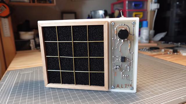
Making A PCB The Old-Fashioned Way
Nearly all modern PCBs are designed with the help of EDA software, but not all of them. [ALTco] shows us the process of plotting out a board the old-fashioned way — by hand. Back in the day, …
Silicon Photolithography The PCB Way
[ProjectsInFlight] has been doing some fantastic work documenting his DIY semiconductor fab lately. Next up: exploring down-and-dirty photolithography methods. If you’ve been following along …
Silicon Photolithography The PCB Way
[ProjectsInFlight] has been doing some fantastic work documenting his DIY semiconductor fab lately. Next up: exploring down-and-dirty photolithography methods. If you’ve been following along …
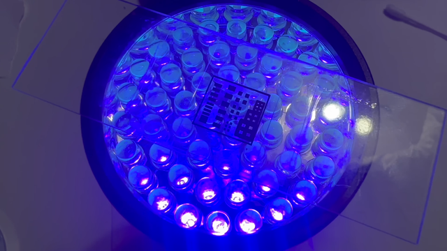
Testing Oxide Etchants For The Home Semiconductor Fab
Building circuits on a silicon chip is a bit like a game of Tetris — you have to lay down layer after layer of different materials while lining up holes in the existing layers with blocks of …

Different Etching Strokes For Different PCBs, Folks
[Sebastian] probably didn’t think he was wading into controversial waters when he posted on his experimental method for etching PCBs (in German). It’s not like etching with hydrochloric…