I've persuaded my SP0256A-AL2 to "sing" the Twelve Days of Christmas.
https://diyelectromusic.com/2025/12/23/sp0256a-al2-sings-the-twelve-days-of-christmas/
#SP0256AAL2 #ArduinoUno #MusicAdventCalendar #MyApologies #FiveGoldRings
I've persuaded my SP0256A-AL2 to "sing" the Twelve Days of Christmas.
https://diyelectromusic.com/2025/12/23/sp0256a-al2-sings-the-twelve-days-of-christmas/
#SP0256AAL2 #ArduinoUno #MusicAdventCalendar #MyApologies #FiveGoldRings
SP0256A-AL2 Sings the Twelve Days of Christmas
Partly prompted by a programming challenge by Futzle on Mastodon, I thought it might be interesting to try to get my Arduino and SP0256A-AL2 to sing the Twelve Days of Christmas.
https://makertube.net/w/diBkzrhkh3tekAPBhGzrVj
Warning! I strongly recommend using old or second hand equipment for your experiments. I am not responsible for any damage to expensive instruments!
These are the key Arduino tutorials for the main concepts used in this project:
If you are new to Arduino, see the Getting Started pages.
Parts list
The Code
I wasn’t aiming for a clever code solution, as can be seen submitted to the programming competition already, but I was hoping to get the computer to do at least some of the work for me.
The first issue is getting a useful range for the song. My original MIDI SP0256 project managed around an octave and a half. Well it so happens that the 12 Days of Christmas is just over 1 octave, so if I can position that to the top end of the range, I should be ok.
This is the most compact notation of the tune that I know of. This is from the “Christmas Praise” Brass Band carol book, which seems to be one of the most common references for any band out caroling at this time of year.
Ignoring the introduction, I’m going to transpose this into concert Bb (i.e. up a minor third) which gives me a note range from F2 through to G3. This allows me to use a sensible range of the SP0256A without it getting too slow down at the bottom end of things.
The main text/lyric structure will be set up in a series of functions as follows:
intro() - "on the nth day of Christmas my true love gave to me"Some variations are required as follows:
In order to capture the variations and repeats for each verse, I’ve opted to use an increasing bitmask for each time through to trigger the various phrases. Bit 0 always indicates one() must be called. Bit 1 indicates two(), and so on. It starts with the value 1 but will keep adding another bit as the verses change, so will have the values 1, 3, 7, 15, 31, 63, etc. thus allowing me to build up the verses with one bit per verse.
one() takes bool parameters to indicate first time and last time through. two(), three(), four() take a bool parameter to indicate if it is a “post five gold rings” verse. Using the bitmask this is pretty easy as it just means any of the bits 0x0FF0 will be set for verses 5+.
Here is the main code loop.
uint16_t phrase=1;The timings were really quite tricky as I have several variables to work to:
In principle I could probably work out the slowest interval and work back from there to get some accurate timings, but I just did a bit of trial and error on each phrase until it was close enough. The unevenness remaining was because I didn’t want to slow the whole thing down to the slowest phrases being “sung”. It is slow enough already!
Also, as it doesn’t look much, I’ve added an LED to light up at the start of an allophone and to go off whenever a pause is encountered.
Closing Thoughts
I’m actually really pleased with this. It is a good balance of close enough to show the principle without me undertaking complex timing and endless fiddling.
I could probably get a bit cleverer with the code, but that wasn’t really the point for me. I’ve used an algorithm where it mattered to me, and was quite happy to spell out the allophones, frequencies, and timings by hand as I went.
Lastly, let me wish you the compliments of the season, to you and yours.
Kevin
Atari Synth Cart Controller
This project uses my Atari 2600 Controller Shield PCB in reverse, to allow the Arduino to act as an Atari keypad controller and thus allow it to control the Atari Synth Cart.
https://makertube.net/w/ryCciwFyQQpcs1Q4Wwy52x
Warning! I strongly recommend using old or second hand equipment for your experiments. I am not responsible for any damage to expensive instruments!
These are the key Arduino tutorials for the main concepts used in this project:
If you are new to Arduino, see the Getting Started pages.
Parts list
The Circuit
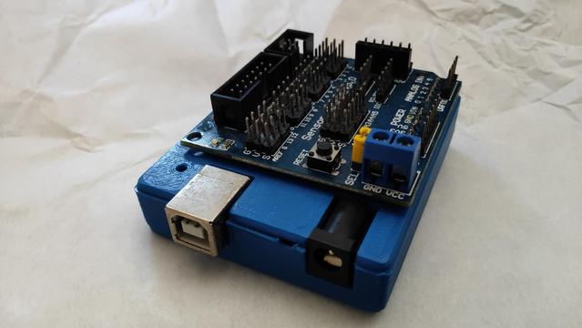
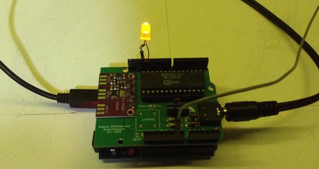
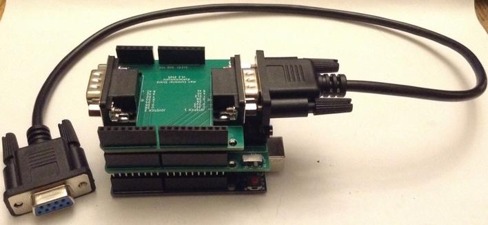
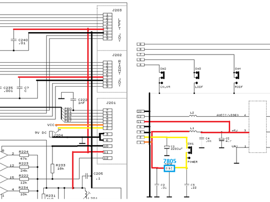
In this use of my Atari 2600 Controller Shield PCB the 9-pin d-type connectors are directly connected to the Atari console.
There is one issue however. Which device should provide 5V? The Atari pinout has 5V present on pin 7 and this is hooked up to the Arduino 5V line.
It may be possible to run the Arduino off the Atari 5V line, which would be really convenient if so. But I’ve not found a definitive statement of the maximum current draw through the 5V pin of the d-type connector from an Atari 2600.
From the schematics for the 2600, it appears that the 5V comes directly from a 7805 regulator. This may or may not go via a single inductor depending on what version of the schematic I’m looking at (yes, for the schematics on Atari Age, below, no for the schematic in the field service manual).
From the BOM in the field service manual, this would appear to be a 78M05 which I believe has a maximum current output of 500mA with a suitable heatsink.
But that has to power the entire console of course. In a not particularly scientific measurement, I believe my 2600 jnr was drawing around 360mA and my “woody” perhaps around 320mA. I don’t know how this changes with different games or controllers.
According to this post, an Arduino Uno with no IO pin current draw, will pull around 50mA when powered from the 5V line directly. Curiously, a bare-bones ATMega328P can apparently drop to almost 15mA when not driving regulators, a USB chip and a power LED…
From powering up a number of Arduino projects I had lying around, most hardly registered on a simple USB current meter using 10mA units. Some with LEDs got to show 0.02A. Some with screens got up to 0.2A.
So just thinking about it in a somewhat hand-wavy kind of way, I suspect that powering an Uno would probably be ok…
If not, then the 5V line to the d-type connectors will have to be cut and the Arduino independently powered. But then the signals for the keypad will be set at the Arduino’s idea of what 5V looks like, not the Atari. They ought to be essentially the same, but it can’t be guaranteed.
Ideally to go this route, the Arduino would isolated from the Atari and be switching the Atari’s 5V line on and off for the input signals as required, but that would require a new design of the PCB.
So time for an IMPORTANT WARNING: This could well damage the Atari 2600 console as I’m essentially making it up as I go at this point.
I have a cheap Atari 2600 junior that I picked up a while back that I’m happy to experiment with. I’m not using my own, original “woody”. In the end I used the following:
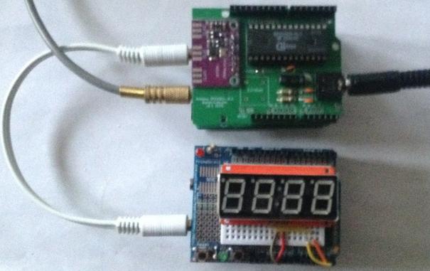
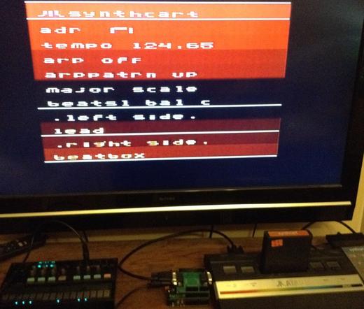
Volca <– 3.5 mm jack to jack –> Arduino TRS MIDI + Atari Shield <– 9-pin to 9-pin –> 2600
Here is the full setup using a Video Touch Pad as the second controller. Note the Arduino is fully powered from the Atari at this point, but the Volca is running on batteries.
The Code
The basic principle for the Arduino is to monitor the Atari’s “row” signals via INPUT pins and when detected drive any OUTPUTs LOW to indicate keys being pressed. The basic algorithm is as follows:
rows[] = IO INPUT pins connected to D-type pins 1, 2, 3, 4
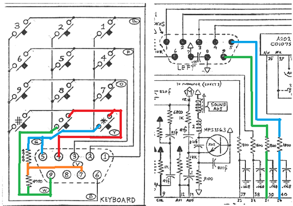
The keypad row/column map was shown in Arduino Atari MIDI Keypad and reproduced here:
Active (pressed) keys will show as LOW in a column when that row is scanned, so to emulate 6 being pressed, when row on pin 2 is detected as being LOW, column on pin 6 should be driven LOW and columns on pins 5 and 9 should be driven HIGH.
I need to map these keys over onto MIDI notes. One issue is that the Atari doesn’t have a natural scale as generating the frequencies for notes is pretty limited.
Still, I’ve mapped the 12 keys, with their non-natural scale, over onto MIDI notes 60-71 – i.e. all semitones up from middle C.
I’m using PORT IO in an interrupt driven scanning routine to ensure the Arduino is as responsive as it can be to ROW scanning. I also pre-compute the actual column bit values when a MIDI note is received, meaning the scanning routine only has to write out the preset values.
The main functions that achieve this are shown below, with the PORT IO values set up for the second Atari controller connector on my Atari 2600 Controller Shield PCB.
uint8_t row[ROWS];As the Synth Cart notes are mostly controlled from the left controller, I’m only coding up for the Arduino to drive one controller. I’m using a genuine Video Touch Pad for the second controller.
Update: The code now includes a controller pass-through mode. If a keypad is plugged into the second socket on the Arduino, then either MIDI or the keypad can be used to drive the Synth Cart.
To achieve this, there are now two sets of row[] arrays containing the column values and when it comes to writing them out, they are combined as follows:
if ((PINB & 0x08) == 0) { // D11As the signals are active LOW, the two values need to be logically ANDed together to get the correct result. I could have simply called the same noteOn/noteOff routines for the keypad, but then I’d have the situation where if both keys for a note are active, the first one released will stop the sound. By combining them in this way, the note will keep sounding until both keys are released.
Closing Thoughts
I really ought to map the pitches of the Atari notes onto their respective MIDI notes, but then I’m not sure what to do for the gaps.
In principle I could wire up both controllers and then use MIDI pads on a MIDI controller just as MIDI-driving control keys rather than actual keyboard notes, but this shows the principle.
I’m still not sure about the power issues, but it seems to work. I guess it will keep working until one day it might not and I’ll be looking for a new Atari 2600 junior.
The slight stuttering in the video is when I end up touching a couple of the volca’s keys at the same time. I suspect I could do something a bit more robust in code to prevent repeat triggering, but this is all fine for now as a proof of concept.
Kevin
TD4 4-bit DIY CPU – Part 7
Once the idea was floated, in Part 6 of creating an Arduino “direct to ROM” assembler, I had to just do it, so this post is a little diversion from the hardware discussion into how that could work.
Basic Concepts
This relies on using an Arduino as the ROM as described in Part 6, but the Arduino now has the option to change the ROM contents independently of the TD4 itself.
The Arduino sketch will do the following:
The code will thus have a number of key sections:
The TD4 ROM routine has already been fully described in Part 6. The only difference is that the scanning routine will be driven from a 1mS timer using the TimerOne library.
As I want to still support a built-in demo, I now have the concept of ROM being the demo code and RAM being the “live” code to pass onto the TD4. The Arduino will initialise the RAM on startup from the ROM.
As far as the TD4 is concerned of course, this is all still ROM.
Command Line Interpreter
The standard Arduino Serial routines will be used to scan for input via the serial port. It will support a line-oriented input as follows:
bool cmdRunner (void) {This will keep adding any received characters to the cmdInput buffer until a newline is received, at which point the command is saved in cmdSaved and the routine will return true indicating a full line is ready to be processed.
Once a complete line is received, then a processing function will parse it.
Key to the processing of commands is a command table that stores the text to match and the handler function to call on finding a valid command. There is an additional parameter that will be passed into the handler function to allow the same handler function to support several commands. This will be used in the assembler itself later.
struct cmd_t {The algorithm for parsing commands is as follows:
cmdProcess:The implementation is a bit complex, as it uses string pointers and has to chop and parse strings as it goes. It is also detailing with the command table in the Arduino’s PROGMEM which is an additional complication too.
In order to be able to use the same command line interpreter for the input of assembler instructions, I’ve had to simplify the syntax. There are no spaces in opcodes and there has to be a space between the opcode and immediate value if used.
Here are some examples:
IN A -> INAHandler Routines
All handler routines have the following prototype:
typedef void (*hdlr_t)(int idx, char *param);The idx parameter is the number in the last field of the command table. pParam will be a pointer to the parameter string for the command (if used).
As we’re dealing with strings all the time, there are a number of helper functions to do things like convert strings to numbers as well as others to print numbers in various formats.
Number formats are assumed to be as follows:
0..9 - decimal digitsThe code provides the following:
The code supports the following commands, so each has its own handler function:
Assembler
As already mentioned, I’m using the same command line interpreter code to create the assembler. To do this, each opcode has an entry in the command table:
const cmd_t PROGMEM cmdTable[NUM_CMDS] = {The order corresponds to the opcode command value, as does the parameter. As these are at the start of the table, I can assume that the position in the table is the same as the command value. This does mean that I also need to account for the duplicated instructions even if I don’t need to use them.
I’m making the following design decisions:
The main logic of the assembler handler is as follows:
Assembler:Disassembler
Disassembly is really largely a look-up table matching opcode command values to text. This is all hidden away behind the two print routines printins() and printop().
void printins (uint8_t ins) {The main complexity is pulling the strings out of the command table. I’ve had to include a macro to provide access to the strings from the Arduino’s PROGMEM:
#define FSH(x) ((const __FlashStringHelper *)x)This feels like a bit of a hack, but apparently this is how it should be done for the kind of thing I need to do!
There is another macro here that needs explaining:
#define HASIM(op) (op==0||op==3||op==5||op==7||op>9)This is a set of conditions that if true means that the command supports an immediate value. This is used in a few places to know how to parse the commands.
Whilst in principle all commands could use the immediate value, the “official” statement of how they work assumes im=0 in many cases. So, for example, OUT B does not require an immediate value, but if one is provided then OUT B becomes OUT B+im.
I’m not really supporting that with this code at the moment.
Putting it all together
Here is a serial output log of a session using the assembler.
> HConclusion
The basics for this actually came together fairly quickly, but I must admit to spending a fair bit of time fiddling about with output formats and refactoring various bits of code to try to give some consistency in terms of when newlines are applied, what is shown in binary, what in hex, and so on.
I can’t guarantee everything has been caught, but I’ve typed in all the code (using the newer, limited syntax) from Part 3 and they all seem to work.
It would be nice to be able to automatically reset the TD4 from the Arduino, but for now, pressing the button when required is fine.
For the most part, unless there is a loop to get caught in, the code will cycle back to the start anyway.
In terms of possible updates and enhancements, there are a few on my mind:
If I expand the instruction set and architecture, then I’ll have to think again about chunks of this code, but for now, it seems to work pretty well.
Kevin
TD4 4-bit DIY CPU – Part 6
Having now successfully built my own version of the TD4 4-bit CPU in Part 5, I’m now chewing over some of the ways I’d like to try to expand it.
I already have a list of others extended projects at the end of Part 4, so I might be drawing on some of them for inspiration moving forward. Many of these are very similar projects, but with a completely different architecture. But really at this stage rather than build a different, more capable, 4-bit CPU from someone else’s design, I’m interested in seeing how far the TD4 design can go. So, ultimately, like all my projects, the fun here is in the reinventing and learning on the way.
One of the questions I have is can I replace the DIP switches with something that can provide the data in a better way? This would be particularly critical if I expand the address space in the future. A ROM is the obvious option, but something more dynamic might be an interesting experiment too.
This post looks at options for replacing the DIP switches with microcontrollers.
Now I feel like I really ought to state right up front that this is a pretty ludicrous thing to do.
At the more charitable end of the endeavor I’m using a 16MHz 8-bit AVR microcontroller with 2kB of RAM to serve up 16 8-bit values to a 10Hz 4-bit CPU.
At the most extreme end I’m using a 125MHz, dual-core, 32-bit ARM Cortex M0+ CPU with 264 kB of RAM running an entire interpreted programming environment requiring (probably) millions of lines of low-level code to implement it, to do the same thing.
So why bother? Well – why not?
TD4 without the ROM
To interface to a microcontroller, I’m after two things:
The best place to get at these signals is on the interface to the ROM itself – the 74HC540 octal line driver, and 74HC154 4-to-8 line decoder.
Conveniently, these signals can be broken out quite easily on my board as shown below.
The pink shaded area shows which components are needed for a ROM-less build. The two yellow highlights show where headers should be soldered to permit access to the address lines (top) and data lines (bottom).
In this build, the following components are omitted from the full board:
I’ve used 6-way and 10-way pin header sockets to allow me to patch in a microcontroller. This allows for each header to conveniently include 5V and GND too. I’ve included the USB socket for power to the PCB but expect I’ll probably power the board via these 5V and GND links from the microcontroller.
Using Arduino
The natural choice here is to use one of the older Arduino boards, as these are all 5V IO which makes interfacing with the 4-bit CPU fairly straight forward.
Using Arduino direct PORTIO should also make it pretty trivial to read address lines and write the data. I’ve configured the connections as follows:
TD4 SignalArduino GPIOArduino PORTIOA0A0PORTC:0A1A1PORTC:1A2A2PORTC:2A3A3PORTC:3D0D8PORTB:0D1D9PORTB:1D2D10PORTB:2D3D11PORTB:3D4D4PORTD:4D5D5PORTD:5D6D6PORTD:6D7D7PORTD:7I’m avoiding D0/D1 (PORTD[0:1]) and D13 as they all have other hardware attached (serial port and LED in this case).
Accessing the data corresponding to any specific address is as simple as follows:
uint8_t ROM[16];The code could be simplified if I didn’t mind trashing whatever is configured for the other GPIO pins via the PORTIO, but it is good practice to preserve those values when only writing to a subset of the IO ports.
In the final code below, I’ve included a toggle for A5 which allows me to do some timing measurements too.
uint8_t ROM[16] = {Running the code in a loop like this gives a scan frequency of around 500kHz and a response time of something like 2-3 uS for each read. That seems pretty responsive and I’m sure will be fine for a 10Hz CPU. And it is – it works great!
Using Circuitpython
One thing that would be really nice is a workflow that allows more of a “direct save to the CPU” approach to programming it. One option is to use a more modern microcontroller that supports a filesystem.
The obvious choice here is a 32-bit microcontroller that supports Circuitpython. But will IO in Circuitpython be fast enough to respond to the CPU? There is one obvious way to find out – give it a try.
There is another complication too – most Circuitpython boards run at 3.3V not 5V so that needs to be addressed too.
Level Shifting
I’m going to use a 74LVC245. The Adafruit product page puts it best:
“essentially: connect VCC to your logic level you want to convert to (say 3.3V), Ground connects to Ground. Wire OE (output enable) to ground to enable the device and DIR (direction) to VCC. Then digital logic on the A pins up to 5V will appear on the B pins shifted down to the VCC logic.”
This is an 8-way bi-directional bus transceiver and should be powered by 3V3, then the direction pin will determine the direction of the conversion as shown[ below.
Two devices will be required. The address lines will need a 5V to 3V3 conversion; the data lines will need 3V3 o 5V.
Here is how I’ve wired these up for a Raspberry Pi Pico:
The Pico is connected as follows:
CircuitPython ROM
The basic algorithm will be as follows:
ROM = [16 command byte values]For performance reasons it would be best to optimise both the reading of the address lines and the writing of the data lines, ideally into a single access. But as this is for a CPU that runs at a maximum of 10Hz, so for now, I’m just going with simple and see how it goes.
import boardI’ve included a timing pin to GPIO21 so I can see how long it takes to access the IO.
It turns out that it takes something of the order of 50-60uS to read the four address lines and something in the region of 70-80uS to write out the 8 data lines. The above simple Circuitpython code to do this is running with a frequency of around 7kHz.
Now at this point I ought to be reading through the datasheets for the ICs used in the CPU to check response times and timing tolerances so see if this is ok. But I didn’t bother with any of that as it all appears to work!
Conclusion
The Circuitpython is obviously a lot slower than the Arduino running optimised PORTIO code, even though the Circuitpython is running on a 125MHz processor compared to the Arduino’s 16MHz. Of course, if performance was critical then switching to direct GPIO access in C on the Pico would be a lot faster again. Even just having a way to do a single block-access of GPIO would probably make quite a difference.
But for this application, either as they are seem to work absolutely fine.
The ability to quickly edit the ROM contents is pretty useful with the Circuitpython. But I am now wondering how difficult it would be to have some kind of uploader to the Arduino over the serial port. There are only 16 bytes to transfer after all.
In fact it might even be possible to create a simple interactive assembler that allows code to be typed in over the serial port using proper word-based op-codes (like ADD, IN, OUT, etc). At the very least a simple serial port interface to type in numeric values would be relatively straight forward I think. It might also be possible to allow the microcontroller to reset the CPU too.
I’m not sure the added complications of logic shifting, etc, make it worth carrying on with a Pico version at this stage, so I think improving the Arduino is probably the way to go for now.
Kevin
#4bit #arduinoUno #circuitpython #portio #raspberryPiPico #td4
I guess I will stick with #raspberrypi 5 for now : https://www.jeffgeerling.com/blog/2025/arduino-uno-q-weird-hybrid-sbc
Hackspace LED Panels
I was lucky enough to get some 16×64 LED Panels in a Hackspace giveaway, courtesy of Limehouse Labs, London, but have only recently started to look at how to use them.
As usual, these are my “notes to self” after attempting to use the suggested libraries and not really getting how they work, so I ended up doing what I often do – reinventing this particular wheel so I really understand what is going on.
https://makertube.net/w/uMhG7dcEs9D5BYmsXF7MVK
References:
And the main devices on the panels are the MBI5034 shift register ICs.
Introduction
The best description of the bit stream required to drive them can be found here: https://wiki.london.hackspace.org.uk/view/LED_tiles_V2
It is a bit complicated…
The general idea is to send the bit pattern for both D1 and D2 at the same time for a specific address (0, 1, 2 or 3) and keep clocking the appropriate bits out to the device. Then change the address and do it again until all four addresses have been covered.
The address isn’t really an address as such – it is more of a matrix “scan line” in that the LEDs are matrixed so that only the LEDS with the common line corresponding to that “address” will be activated at any one time. As there are four lines, the whole panel can only be scanned using persistence of vision, illuminating each scan line in turn.
To drive multiple panels means adding their D1 and D2 lines to the system too, but sharing all other signals. Most approaches I’ve seen encode all 8 bits or each of the eight Dn lines into a single byte and then sent those out in parallel to four panels at the same time.
If the data is stored in a frame buffer in “4 panel Dn ready format” then driving four panels isn’t really that much slower than driving one.
Some numbers:
So on that last point – as already mentioned, the 74HC138 8-line decoder links the address lines A0, A1 to four outputs (Y0, Y1, Y2, Y3). This is used to “select” one of four blocks of 16 LEDs per MBI5034. Once each address has been scanned, each MBI5034 can be seen to be driving the equivalent of 4 rows of 16 LEDs in total, which is the required 64 LEDs each.
Apparently each MBI5034 will directly address a single LED colour: R, G or B. So 48 of these, driving 16 R, 16 B, 16 G means they can directly address 768 LEDs, or 256 R, G, and B LEDs. Again, doing this four times gives the full 1024 RGB LED panel.
This all means that the panel is logically arranged as two 128 x 4 matrices, physically arranged across two rows of 64 LEDs each. The full 16 rows of 64 LEDS are selected by the following combinations of D1, D2, A0, A1:
A0A1D1 = 1D2 = 100Rows 0, 4Rows 8, 1201Rows 1, 5Rows 9, 1310Rows 2, 6Rows 10, 1411Rows 3, 7Rows 11, 15A further complication is that each row itself is encoded not as 2 sets of 64 RGB values, but as 8 sets of [16-bit B + 16-bit R + 16 bit G] values with the 16-bit B, G, R values encoding 8 of each colour LED on the first row, and then 8 on the second row.
The upshot of all this is that 384 bits of data must be streamed out to the shift registers for each address, but only two lines per half-panel can be illuminated at any one time. As I say, persistence of vision is required to illuminate the entire panel.
The basic algorithm required to display something on the panel will thus be as follows:
FOR EACH bank (address = 0, 1, 2, 3):Hardware
I had some of the interface PCBs made, that were described here: https://github.com/limehouselabs/led-screens/tree/main/panel-connector
The central block is mapped over to a JST PH 8-way connector as follows:
D1LATA1N/CD2OEA0CLKJST PH Connector:
The board provides screw terminals for a higher current 5V supply.
Various estimates suggest one panel could require up to 8A with all LEDS on at full brightness, so I’m using a 40A 5V supply. The main issue is ensuring the Arduino’s GND and the GND of the power supply are linked, which this PCB does.
Arduino “Shield”
After getting fed up with jumper wires falling out of solderless breadboards, I eventually soldered up a simple Arduino proto shield able to support up to four panels.
This maps the panel signals onto Arduino pins as follows:
ArduinoPanel(s)A0A0 (all panels)A1A1 (all panels)A2CLK (all panels)A3LAT (all panels)A4OE (all panels)D4D5 (D1 panel 3)D5D6 (D2 panel 3)D6D7 (D1 panel 4)D7D8 (D2 panel 4)D8D1 (D1 panel 1)D9D2 (D2 panel 1)D10D3 (D1 panel 2)D11D4 (D2 panel 2)The slightly odd mapping of Arduino digital outputs to panels will become clear when we look at the code.
Using this with a ready-made JST PH connector-to-jumper-wire cable and then crimping Dupont header pins onto it seems to do the job (or so I thought).
Driver Code
I started with the Arduino code linked to above. This is written for an ATMega32U4 based Arduino and uses direct Port IO to access the panels.
I wanted to use an Uno or Nano, so I started to port this over to an ATMega328, but just could not get anything working at all, so in the end I decided to go back to basics and rewrite the code from first principles so I knew what was going on.
The basic design of the code will be as follows:
Driving Four Panels at Once
All signals apart from D1 and D2 are common to both halves of each panel. This means that once the code has processed the address signals, LAT, CLK and OE, there is no reason not to then process D1 and D2 for all existing panels in parallel.
This can be done pretty efficiently on an Arduino by mapping the eight Dn signals onto a single Arduino port and using PORT IO to write out all four values at once.
It isn’t quite that simple however, as there isn’t a single 8-bit port on an Arduino that isn’t used for something else too, so I’m going to do it in two halves, using PORTB and PORTD as follows:
Panel DnArduino DnArduino PORTP1 D18PORTB 0P1 D29PORTB 1P2 D110PORTB 2P2 D211PORTB 3P3 D14PORTD 4P3 D25PORTD 5P4 D16PORTD 6P4 D27PORTD 7Using this mapping, an 8-bit value can be stored in the framebuffer per LED as follows:
b7 6 5 4 3 2 1 0And then when it comes to writing it out via the Arduino digital IO it can be done in two instructions:
PORTB = (PORTB & (~0x0F)) | (data & 0x0F);This is mapping the low 4 bits of the data value onto the low 4 bits of PORTB and the top 4 bits of the data value onto the top 4 bits of PORTD.
The Writing Protocol
Implementing the protocol described in the various references, I’m after the following basic structure:
The entire routine for updating the display is as follows.
void panelScan (void) {This processes a single address per scan, so four scans are required, with persistence of vision, to illuminate the entire display.
The various macros, such as CLKSET, CLKCLR and so on, are defined for individual bit manipulation PORTIO as follows:
#define CLKSET {PORTC = (PORTC & (~0x04)) | 0x04;} // A2SETADDR is a special macro that sets both A0 and A1 at the same time.
#define SETADDR(x) {PORTC = (PORTC & (~0x03)) | (x & 0x03);} // A0/A1setDataOutput() is an inline routine that has the two previously mentioned lines in it to set PORTB and PORTD.
The Framebuffer
There is one unexplained item in that previous routine. The value passed into setDataOutput is an entry from the frame buffer – the “panel ready data format” I mentioned previously.
Here is my description of how the framebuffer works from the code itself followed by my setPixel routine that implements it.
// The panel is addressed as a string of bits, representing 64 R,G,B values.Understanding how the y value turns into a panel, Dn, and An number is perhaps best shown with an example. The following shows how incrementing the y coordinate maps onto panels.
y=b7654 3210 A D P1Following the x coordinate mapping is ok once the idea of using the coordinate value to orient to the start of the 48-bit triple of 16 B, 16 G and 16 R values across the two rows is figured out. Then it is a case of calculating the offset within the referenced 48-bit triple as per the comments in the code above.
Set Brightness
There is a special command word that can be used to set the overall brightness of the driver chips. Sending this to all 48 chips on a panel will set the brightness for the whole panel.
Full details can be found in the “dimming the panel” section here: https://wiki.hackhitchin.org.uk/index.php?title=LED_panel_interface and in the MBI5034 datasheet (see “Current Gain Adjustment”).
This is the brightness function:
void setBrightness (uint8_t brightpercent) {Notes:
There is one added complication though – whilst this is going on, the normal scanning should be paused to ensure it doesn’t interfere.
Strictly speaking, the setBrightness routine should pause briefly too, to ensure any existing scanning is complete, but as the interrupt is higher priority than the running code, it should always complete first anyway.
Code Summary
I’ve ended up with the following routines in my code:
void panelInit (void);To use these requires the following basic setup:
#include <TimerOne.h>Notes:
Find the full code on GitHub here.
Expanding to Four Panels
When it came to it, wiring up four panels wasn’t going to work with the cables and shield I already had, I would have had to have made some longer ones, so in the end I just soldered up a slightly different arrangement of the Arduino shield.
I’ve also added some screw terminals to allow the Arduino to be powered directly via its 5V pin from the main 5V power supply to the panels. I’ve added a 220uF capacitor to attempt to give some stability to the power as the LEDs turn on and off.
I experimented with some 3D printed connectors but couldn’t get anything that connected snugly enough to keep the panels together, so in the end just nailed four panels to a piece of wood as shown.
I have test code for the following:
I wasn’t able to capture the “all pixels on” Mandelbrot without the scan lines becoming apparent. I’m not entirely sure why this would be different compared to when it is building up the set or running the Game of Life, but it does. I’ll have to have a think about that one!
Also, I don’t have enough memory on an Uno for a full dual-buffer grid for the Game of Life, so I’m using the pixel buffer itself as the state of the “live” display and have another buffer to calculate the updated values. To have all this on an Uno, I’ve had to limit the display to 52 rows rather than the full 64. Even that only gives me 62 bytes free!
Update: the latest version of the code includes an option to fade dying cells out using different colours. This is shown in the video at the start of this post.
Other Notes
It took me ages to get this working – almost a week on and off. I tried everything – checking the protocol with a scope; working through the interrupt performance and timing requirements; dropping back to a simple test case; ultimately soldering up that interface board and verifying the power supply. I even went right back to first principles and coded up my own routines that I could fully understand.
But I couldn’t get the panels to work.
In the end I took one panel apart and started poking around with an oscilloscope.
Interestingly there are two HC245 line buffers directly off the interface connection. One appears to produce four OE lines and four CLK signals. The other appears to have the address, data and other signals.
It turns out that my crimped connector had a dodgy link on the LATch wire, so although I could see all the correct signals happening at the Arduino end, the LAT signal was never actually making it to the panel!
That will teach me to check first principles and not assume anything.
Or rather, I suspect it won’t and I’ll continue to have plenty more similar issues as I move forward.
As usual a massive thanks to those who have worked out how to do all of the above, and a big thank you to Limehouse Labs for the large giveaway in the first place!
Kevin
Arduino AY-3-8910 Shield Build Guide
Here are the build notes for my Arduino AY-3-8910 Shield Design.
Warning! I strongly recommend using old or second hand equipment for your experiments. I am not responsible for any damage to expensive instruments!
If you are new to electronics and microcontrollers, see the Getting Started pages.
Bill of Materials
If both chips audio outputs are to be combined, using the solder bridges, then only one 1uF electrolytic capacitor should be used.
Build Steps
Taking a typical “low to high” soldering approach, this is the suggested order of assembly:
There are two solder bridge jumpers which can be used for the following:
By default, one chip goes to the left audio output and one goes to the right, but it is possible to combine them into a single mono output. But then there is another choice: combine the left and right audio channels (tip and ring) for the TRS socket; or leave all outputs just to the tip of the socket.
If these options are being considered, then one of the output electrolytic capacitors should be omitted too. More details below.
Here are some build photos.
The ceramic capacitors are actually shown as being installed on the underside of the board, but depending on the 40 pin DIP socket used (or not) it may be possible to install them on the top side of the board as I’ve done below.
I’ve used “extended headers” which give me a breakout for the Arduino GPIO on the top of the board. If simple pin headers are used, then care should be taken about the height of the board and avoiding the possibility of the resistors shorting out on the USB socket of the Arduino.
Solder jumper options
For mono operation:
For mono socket operation, i.e. TIP and GROUND only, leave the solder bridge highlighted in ORANGE unbridged. This allows a mono jack lead to be used as RING is unconnected in the socket and can be ignored.
To take the mono signal into a stereo socket, i.e. TIP, RING and GROUND but with TIP and RING having the same mono output signal, solder the bridge highlighted in ORANGE. This allows a stereo jack lead to be used and both channels will received the same output signal.
Testing
I recommend performing the general tests described here: PCBs.
Once everything appears electrically good, a variation of the test application from my AY-3-8910 Experimenter PCB Build Guide can be used that will play a chord on both of the devices at a different octave.
Note: the GPIO usage of the Arduino is printed on the back of the PCB and listed in the Arduino AY-3-8910 Shield Design.
PCB Errata
There are no known issues with the PCB at present.
Enhancements:
Closing Thoughts
This seems to work fine and is a lot simpler than my quad board if some simple experimentation is required.
I still haven’t gotten around to building some real applications for any of these boards yet though, so ought to get on to that.
Kevin