An alternative to packaging chips is to do 'chip on board', where you glue the die down and then wire bond it to the PCB.
We just tried this with one of my Zero to ASIC course ASICs, and it worked!

An alternative to packaging chips is to do 'chip on board', where you glue the die down and then wire bond it to the PCB.
We just tried this with one of my Zero to ASIC course ASICs, and it worked!
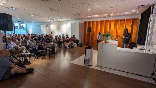
It's official! Teardown will be returning to the mall in June 2025 and @crowdsupply is still letting me run it.
Keynotes will be Cory Doctorow (author, activist), Kate Stewart (VP of Embedded at Linux, Zephyr, RTOS) and bunnie Huang (hardware hacker, author).
We have talks, workshops, hacker art, soldering, synths, SDRs, VR, machines galore, local food, after parties & A+ dying mall vibes.
Early bird tix are on sale and calls for proposals/volunteers are open!

We need more of this in our news.
Something I should have tried out sooner, making use of the USB 3.0 parts of the luna USB stack on the ButterStick FPGA board.
Spun up a simple breakout with a PD controller and data lanes connected to a Type-C.
The LUNA SS code has some bitrot for ECP5 support, but did manage to get it enumerating over the weekend! 😍
All accomplished using the ECP5's built-in 5Gbps serdes blocks and fantastic opensource tools: nextpnr+Yosys, amaranth and LUNA gateware. 🥳🙌🌺


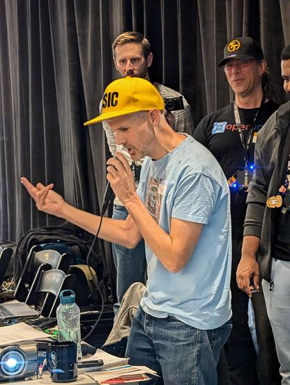
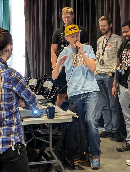
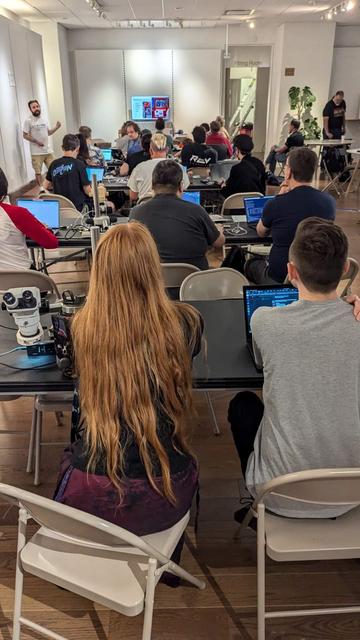
Get started with open source ASICs!
https://www.zerotoasiccourse.com/post/get_started_with_open_source_asics/

In my recent video Getting started with open source ASICs, I provided an overview of the open-source silicon movement, highlighting key resources and tools while showcasing some inspiring projects. The video starts by looking back at the game-changing moment in 2020 when Google, Tim Ansell, and Efabless announced their free shuttle program, making it possible for anyone to get their open-source chip designs manufactured. This sparked a wave of innovation, with many taking their first steps in ASIC design using open-source tools like OpenLane and the Skywater 130nm PDK.