tried to run the toroid off of my beefier bench supply and blew a mosfet.
It's looking like the driver is probably drawing a lot more current than simulated. The miniware psu (and the USB-PD supply) I used yesterday handles brownout pretty gracefully, but I suspect the bargain bin bench PSU is less graceful.
Part of the higher power draw could be due to messy switching, but if I lower the primary cap values in the sim to 66pF (from the nominal 99pF) I get results more similar to the observed circuit. I don't think the frequency or temperature is high enough to cause that kind of de-rating but who knows, could be as simple as one of the three capacitors has failed.
Going to order some more caps, this time explicitly marked as low-ESL.
Still not sure what's up with the coil getting blazing hot.
...not the exact capacitors I have installed, but similar.
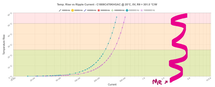
Using a bank of only three is *definitely* asking too much, even if I think things aren't quite as bad as 300°C/W. Note the log scale on x-axis.
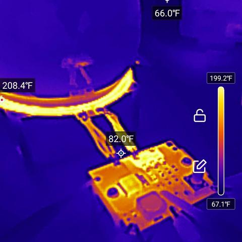
Sincerely though, does anycritter have ideas on why the two-turn 1.9uH PCB coil gets so dang hot?
According to the saturnPCB calculator / IPC 2152, I'd expect less than 30°C rise to steady-state even taking skin effect into consideration, based on my ltspcie sims expecting ~12 peak amps at ~13MHz (sinusoidal).
I see like 70°+ temperature rise within a minute.
Guessing there's something going on with inductor energy getting dumped as heat, so resistive load calcs go out the window. But I have no idea how to reason about those possible effects.
lol so ended up just using I^2 *R just given DC resistance of a few tenths of a ohm and amperages in the 6-10A range...
that's multiple tens of watts of heat.
Very rough estimates of thermal mass give many degrees per second rise.
...yep there's a problem.
So the standard trace width calculations just aren't remotely applicable here apparently!
I now slightly better understand why other folks haven't used PCB inductors here.
I suspect I might still be able to donut with much lower amperages though! If I get down below 3A in the inductor, that's only like four watts heat rather than dozens.
https://hackaday.io/project/194683-plasma-toroid-sky-guided-pcb-edition/log/227533-i-would-like-my-circuit-to-not-cook-itself
i would like my circuit to not cook itself | Details | Hackaday.io
<p>First Light accomplished. What did I learn?<br><br>The circuit in its current iteration,<br>1: gets hot alarmingly quickly<br>2: is trying to draw more power than I can actually supply. <br><br>Those seem related, yeah. <br></p><figure><img data-src="https://cdn.hackaday.io/images/6280501708053920075.jpg" class="lazy"></figure><p><em>apologies for the excessively american temperature units<br></em><br></p><p>Based on simulating the circuit in the condition tested, at 15 volts supply I'd expect to see something like 50W power draw, at around 3.5A. The tests discussed in the previous post sure looked like the USB-based bench supply was badly voltage sagging, so the next day I hooked up the beefier bench supply -- and very quickly started sagging, then blew another mosfet. I <em>suspect</em> that this very-budget bench supply has some sort of destructively un-graceful switch from constant-voltage to the constant-current mode it failovers to when it hits 5A, but it's also entirely possible that the mosfet blew first and I saw the power supply feeding a shorted chip. <br><br>My power budget is <5A @20V (the 100-watt maximum of USB-C-PD), but I'd prefer to stay <60W if possible.<br><br>If I simulate a lower primary capacitance (e.g. 66pF instead of the as-built 99pF), power draw is dramatically greater <em>and</em> the higher resonating frequency is also a closer match to what I observed on the
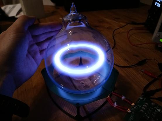
More progress on the plasma toroid! More videos! Less overheating!!
Writeup at https://hackaday.io/project/194683-plasma-toroid-sky-guided-pcb-edition/log/227790-tweakin
Higher-quality vid at https://www.youtube.com/watch?v=rEc76ckTJcg
tweakin' | Details | Hackaday.io
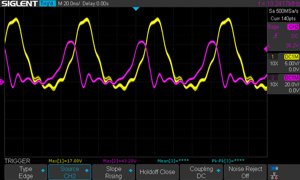
<p>Spent a big chunk of the weekend adjusting a variety of component values. <br></p> <figure><img class="lazy" data-src="https://cdn.hackaday.io/images/7189551708888806047.png"><br>Here's the waveforms with the circuit unloaded (no toroid), at 18V supply:<span></span></figure> <figure><img class="lazy" data-src="https://cdn.hackaday.io/images/2465921708889099062.png"></figure> <p>Yellow is Gate (5V/div), purple is Drain (50V/div), blue is feedback network bias input at TP5 (5V/div).</p> <p>Looks decently healthy to me. I suspect that the gate protection zener diode is doing its job and helping to keep drive voltages within operational limits.<br><br>Here's the traces when the xenon is fully toroid-ing:</p> <figure><img class="lazy" data-src="https://cdn.hackaday.io/images/1735241708891968601.png"></figure> <p>Hm. Clearly the device is overall functional but these waveforms aren't as clean as I'd prefer. Maybe it's fine?</p> <p><br>All right, so let's walk through the component changes. I'll spare the step-by-step of each individual test -- most of it was poorly documented and I was going for more of a "better or worse?" approach than robust characterization. <br><br>First off, primary tank capacitance was increased 99pF to 141pF. This was the first change made, as planned in previous project log "<a href="https://hackaday.io/project/194683-plasma-toroid-sky-guided-pcb-edition/log/227533-i-would-like-my-circuit-to-not-cook-itself" target="_blank">i would like my circuit to not cook myself</a>". <br><br>Increasing capacitor value was broadly successful -- overall power draw was reduced to ~2.9 - 3.2A depending on circuit configuration. Yay!<br><br>Decoupling cap C4 was removed because it caused some kind of runaway oscillation on
More plasma toroid progress! Things are going super well!
Video demo:
https://youtu.be/fBrOaj5pBa0

Plasma Toroid WIP demo #3 - ✨😇
I'm at a point where I could call this "done" if I wanted.
It's not done yet though ^_^
roflll, I'd been working hard to implement a subcircuit for monitoring current draw to indicate out whether or not the primary inductor was in oscillation, using a shunt resistor + op-amp + comparator etc.
And just now realized I can do the same thing *better* using nothing but a loop of wire and an LED.
Plasma toroid project writeup has been updated, with details of the non-contact indicator light shown in the previous video clip.
"status LED, galaxy brain style"
https://hackaday.io/project/194683-plasma-toroid-sky-guided-pcb-edition/log/228373

status LED, galaxy brain style | Details | Hackaday.io
<p>Since a key goal of this project is to run standalone -- no o-scope, no bench PSU, no amperage panel meter -- it's crucial to have some sort of indication of whether the circuit was in oscillation or just sitting idle.<br></p> <p>Overall power draw reliably reflects the circuit's state. When not oscillating, there's near zero draw -- just LEDs, leakages, etc. While running the draw is more like 2-3 amps, and can be reduced down to as little as ~1.2A by lowering mosfet gate bias. </p> <h1>The normal approach</h1> <p>I had initially planned to use the pretty typical current monitoring method of a differential op-amp measuring voltage across a low value shunt resistor. Since I'm looking for a threshold current indicator rather than a continuous analog signal, the op-amp is fed into a comparator, against a reference voltage.<br></p> <figure><img class="lazy" data-src="https://cdn.hackaday.io/images/3954551711072740439.png"></figure> <p><em>Yes, this diagram is kind of sloppy, but you won't need to linger on details here anyway. If the text is unreadable due to aliasing you can click to embiggen.</em></p> <p>The TSM102 IC seemed like a neat combo-wombo of packaging two comparators, two op-amps, and a 2.5V reference all in one. It's also relatively inexpensive and can run off of a 40V Vcc. Purpose-built current monitor
ANOTHER plasma toroid project update: Pushbutton Arc Start!
https://hackaday.io/project/194683
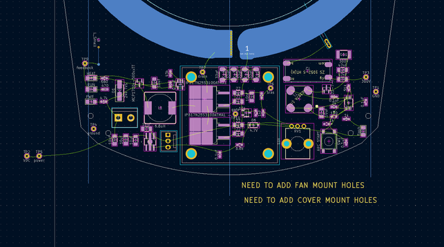
This one is a big deal, since I've now hit every core functional milestone. The next steps are putting all of the subsystems together into a single, unified board.
This subcircuit is also neat because it uses multiple different bits of antiquated technology: photo-flash trigger circuits and gas discharge tube surge arrestors.
(demo vid attached here; high-quality available on youtube https://youtu.be/Vi6Pb0WSCZw )

Plasma Toroid (sky-guided PCB edition)
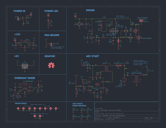
status: v0.1 failure (mosfets destroyed: 5) v0.2 success v0.3 better performance Mission: Create an inductively coupled plasma toroid in a globe of xenon gas. The end goal is to have all electronics (including primary inductor) part of a single PCB running on USB-C-PD power, in a well-built and aesthetically attractive presentation. Inspired by "perfecting and explaining the plasma toroid" by BacMacSci https://www.youtube.com/watch?v=GbMAvn7nRWo The driving electronics is a "class E" self-oscillating circuit based on a SiC MOSFET. A ~2µH loop inductor is driven at 10-15MHz and >2kV, creating a strong electromagnetic field. If a 1-liter globe of ~15 torr xenon is placed in the middle of the inductor, the xenon will ionize into a conductive loop analogous to the secondary winding of a transformer. based on the work of Steve Ward and BacMacSci.
Like I spent literal hours today trying to pick out a heatsink.
Digikey has literally one hundred *thousand* heatsink SKUs from one vendor, and they're all permutations of solution space for the same basic design.
Neither digikey parametric search nor the manufacturer website narrowed things down very well. Even after several different dead ends to figure out what I actually wanted, I basically had to manually decipher the under-documented way this mfg was assigning model numbers.
At long last I am getting to the "finishing touches" stage of this design.
Mechanical CAD is already done.
Btw: plasma toroid is still being very actively worked on! I did a circuit/board integration test "off-camera" because the prototype is very nearly identical to what the final version will be, but lacking in just a bit of ✨ sparkle  that I want to publish fully-formed.
Currently waiting on another round of overseas PCB fab which I expect to take a couple weeks.
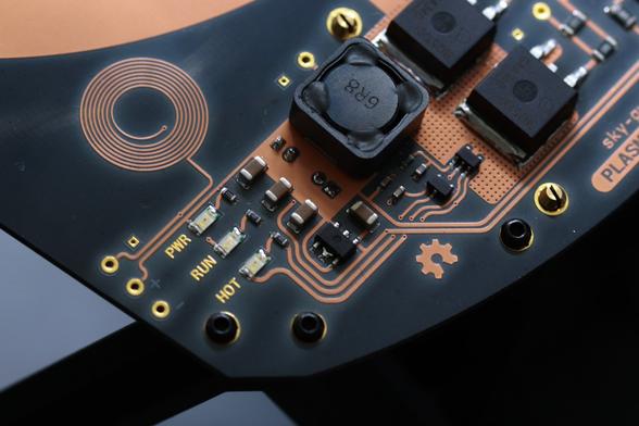
Feature added since my last update: overheat indicator light
(plus it runs cooler in general.)
So I said last update that I was gonna be doing a li'l something special for the final version of the plasma toroid board.
Here's the something special ✨
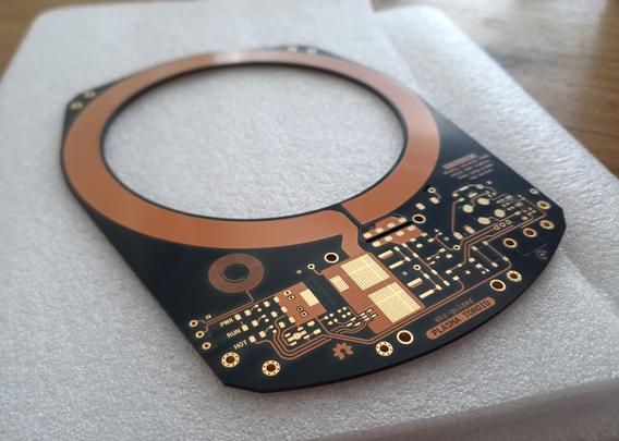
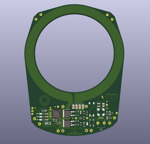
This is a board with dyed-black FR4 fiberglass and transparent soldermask (the layer that's traditionally green).
Not necessarily a *reasonable* expenditure but, woah.
Roadmap for Done is basically:
- assemble
- take good photos (Friend With a Macro Lens is out of town rn...)
- shoot a project video (probably a yak stack in its own right)
- so much writeup
- edit video...
Plasma toroid writeup updated
https://hackaday.io/project/194683-plasma-toroid-sky-guided-pcb-edition/log/230046
"#8: A Unified Board"
#8: A Unified Board | Details | Hackaday.io
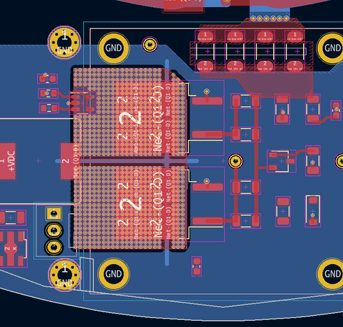
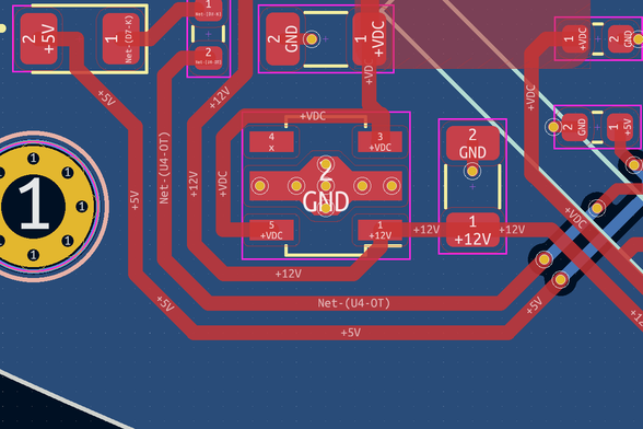
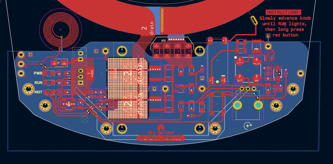
<p>It's been a busy couple of months behind the scenes -- this project is basically finished! I'll be breaking the final few updates into a couple posts, while I wrangle loans of camera equipment for the beauty shots. </p> <h1>Circuit Unification</h1> <p>Taking the different prototyped modules and banging them together:</p> <figure><img class="lazy" data-src="https://cdn.hackaday.io/images/4564281716833141406.png"></figure> <p><em>(you might have to click to embiggen)</em><br>I've paralled the mosfets for better heat dissipation. This doesn't help quite as much as one would like (since a lot of the losses are switching and not resistive), but it does help. The mosfet gate resistors are also paralled since they get <em>quite</em> hot before the arc is struck. I'm not sure why that behavior is occurring -- if you know, drop me a line!<br><br>The 4.3V zener diode (D5) for regulating gate bias is a carefully chosen value for this particular mosfet and circuit. Cranking the knob full-clockwise guarantees oscillations start, but doesn't set the bias so high as to cause excessive power draw and heating. The use of full knob range also makes adjustments more precise and controllable.</p> <p>A bank of four 33pF capacitors is a balance between heat distribution and board space. While the board itself has plenty of room (see below), I ran into
Plasma toroid writeup updated, with something a bit different:
an in-depth look at black-core FR4 and transparent soldermask PCB stackup, sponsored by PCBWay
https://hackaday.io/project/194683-plasma-toroid-sky-guided-pcb-edition/log/230233
#9: Black FR-4 and transparent soldermask, by PCBWay | Details | Hackaday.io
<p>For the final build of this project, I wanted something special.</p> <figure><img class="lazy" data-src="https://cdn.hackaday.io/images/1192521717273710046.jpg"></figure> <p>Typical PCBs use a olive-green fiberglass core, layers of copper, and a (traditionally green) soldermask layer to protect the copper and define areas where solder/component pads should stick. This board instead has a dyed-black fiberglass core and a transparent soldermask layer. This means that all traces are visible as their natural copper color, which is delightfully high-contrast against the black substrate. Component pads and other areas left uncovered by the transparent mask are plated (ENIG) gold. <br><br>This order of circuitboards was <em><strong>(partially) </strong><strong></strong></em><strong>Sponsored by <a href="https://www.pcbway.com/" target="_blank">PCBWay</a>! </strong>They covered about 60% of the cost of these boards, and I paid the remainder out-of-pocket. <br><br>There's <em></em>very few photos out there of real PCBs made using this stackup, so I'm taking the time to write out a review. <br><br>(Transparency: being partially sponsored will likely bias my opinions, but I did also pay enough to feel like I have skin in the game. I have not given PCBWay any editorial control and they will not have seen this review prior to publication. Photos have been lightly post-processed and are broadly representative of how things look irl under good lighting. An order number [visible on the unpopulated
UPDATE:
I've finally released KiCAD source files for the plasma toroid driver.
still need to flesh out documentation.
video status is: still need to shoot one more bit of pick-up footage, do a bit of polish on graphics, finalize the edit, sound cleanup, color grade.
So coming a lot closer to done, at last.
me: "I think this edit is done, including color grade! Just gotta check the rendered output..."
me: "whelp, there's a whole-ass paragraph I forgot to include in the cut. So I'm still not quite done."
AND IT IS DONE
"A plasma toroid for the modern era."
https://www.youtube.com/watch?v=Bl3zHuih_CY

A plasma toroid for the modern era.
Added a proper BoM to the plasma toroid project files
https://hackaday.io/project/194683-plasma-toroid-sky-guided-pcb-edition/files
I also wrote up a quick post to consolidate the "stuff I know I could have done better" thoughts into a single place :)
https://hackaday.io/project/194683-plasma-toroid-sky-guided-pcb-edition/log/232417

#11: Design deficiencies, and what you can improve | Details | Hackaday.io
<p>I'm considering this project Completed, at least for the time being. I'm <strong><em>incredibly</em> </strong>proud of what I've created -- every design goal was achieved, and it looks even better than I'd dared to hope. <br><br>However, this is far, far from perfect. If I were to continue this project, I have a real hit-list of what could be improved.</p><h1>Overall System</h1><p>The biggest issue is that controlling drive intensity by adjusting mosfet feedback bias voltage is janky and unstable. A proper system would leave a bias voltage set with a trimmer, and use high-side limiting on the primary input current for primary drive control. I realized this kinda late in the design process, and wanted to reach "done" rather than do another round of prototyping.<br><br>Also, having a breakout board for the USB-PD trigger module is pretty inelegant. Having a trigger module on-board would be better, but when I started this project I was having trouble finding a suitable IC with decent availability in the US. Several folks have since suggested good candidate ICs. </p><h1>MOSFET and driving</h1><p>A straightforward error is that the gate-drive resistors have been undersized. The design shown in the video uses two 10-ohm 1206-size resistors in parallel (per mosfet), and they get incineratingly hot if
Someone ordered and built one of my boards, and I'm getting some great feedback highlighting differences between "works good on the bench" and "is robust enough for production."
-- they had a short-to-ground through the heatsink, which I find odd given the thermal interface is spec'd as highly insulative.
-- Some of my clearances on the xenon striker were too low and they got arcing under the trigger transformer. I issued a quick board revision to hopefully improve that for anyone else.
[continued]
What has me a bit stumped is that when they added a 330uF capacitor at the power input, one of the switching mosfets (Q1/Q2) will consistently and immediately fail short when the toroid forms.
I'm not sure why that'd happen and I'm very interested to hear y'all's thoughts. Best guess is that without the cap I'd been getting some manner of protective voltage sag at turn-on?
If any of y'all have insight I'm all ears.
re-posting the diagram for reference -- in my build I'd had a total of 30uF X7R bulk capacitance. The physical board is fairly compact, for the switching speeds in question.


Genuinely love PCB layout. Deeply satisfying to start with a tangled mess of components and ending with a board that's both functional (🤞) and nice-looking.
Not architected by any grand plan either, just a bunch of micro-iterative improvements over the course of a couple hours.
Trying to give wantonly generous spacings for inevitable bodge and re-work shennanigans.
New arc start module, bench test.
Not bad for a caveman-simple flyback. ~9mm arc. That's absolutely plenty.
Haven't 'scoped it yet (because bedtime) but should be very roughly 60khz.

Adjustable current-limiting buck converter module: successful.
TI's "simple switcher" family integrated circuit is a little expensive ($2.33USD each) but y'know what that really was simple.

also I spent about an hour trying to figure out why the IC was instantly overheating
gals, turns out I fried the first chip because it was soldered on backwards.
Writeup on the new adjustable current limit for the plasma toroid:
#12: v2, current control | Details | Hackaday.io
<p>After a year away, I'm returning to this project. It's time to come back and fix the deficiencies of Version 1.<br><br></p> <h1>The Problem</h1> <p>Version 1 of the plasma toroid controlled drive intensity with a potentiometer that adjusted oscillator mosfet bias voltage, which in turn changed the switching duty cycle. This isn't a great method of control. Changing the duty cycle introduces a variable phase delay which is harder to tune for. Also, since the drive is a sine wave running a low duty cycle leaves the mosfet in an intermediate half-switched state for longer, which isn't great for efficiency. Finally, low duty cycles would often result in loss of oscillation if the plasma was extinguished for any reason.<br><br>The better method is a dynamic high-side current limit. </p> <p>I'm accomplishing this with a buck converter based on TI's "Simple Switcher" line of ICs, specifically LMR14030SDDAR. This chip is a monolithic buck converter with integrated mosfet, and it really is simple to implement. It's also capable of running at up to 97% duty cycle which is perfect for a low minimum dropout. Here's the reference circuit from their datasheet:</p> <figure><img class="lazy" data-src="https://cdn.hackaday.io/images/6500541758392745491.png"></figure> <p>This is a perfectly normal buck converter topology. Most buck converters are designed to hold a fixed

-F
@skyguided TI also has a number of really handy, not *too* expensive switchers with integrated inductor, too. we've used them a couple times and they're really nice, smaller on the board than we can usually manage manually
the TPSM6360x series will get you huge amounts of current in like a square centimeter, with an enormous input range
-F
@skyguided https://www.ti.com/lit/ds/symlink/tpsm63608.pdf datasheet if you're interested
this specific one is like $15 each but lower current ones are cheaper
-F
-F
-F
@skyguided Probably a drain short then (which usually causes a gate short to form shortly afterward, while a gate short doesn't tend to do anything to the drain)
That indicates likely over-power, operating outside the MOSFET's SOA
-F
-F
-F
-F
@skyguided Fuck yeah nice work!!!
Really dig the thorough explanations! I love how the starter mechanism is basically just a xenon flash circuit because, well, the whole thing is like "what if a xenon flash tube, but bigger, and then we started wiggling it constantly" hehehe 
(the fox mask is cute too!!)
@skyguided Oh my GODDDDD WHAT 😱✨ holy crap bookmarking to watch later
That's freaking gorgeous