presenting without elaboration
best hope that this design is solid, because the board and components are getting ordered rn
that 1k through-hole resistor is there becaussse it was either have a resistor do double-duty as a jumper wire, or switch to a four-layer board just for one trace.
not a good solution but maybe the least-bad.
update:
realized wait, LTspice can totally calculate power dissipation; I ought to see if my components are gonna cook.
fine: MOSFET drawing somewhere like 12-15W which is A Lot but I planned for a heatsink.
probably not-fine: >10W on an 1808 capacitor, 400mW on a 0603 resistor
🌶️ ♨️ 😅
prototype board for only run short durations i guess
me: i need to think very carefully about this board layout and I want things to be clean as possible.
other folks, with apparent success:
(and I'm running way less power than that)
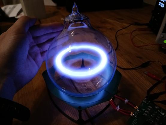
The field-wiggler is operational, at least partially.
Pictured: wirelessly lighting an ampoule of neon.
Problems:
- getting some higher frequency noise on the mosfet gate, probably some sort of parasitic resonance. May or may not be significant.
- drive coil gets *really* hot, fast. 18ga wire apparently isn't adequate for this much RF power?
- I've blown up three out of my five mosfets (and that's not an inexpensive component). Worse, I'm not sure exactly *why* they've failed.
Also I'm still waiting on my larger xenon globe.
Right, of course, my intuition for "how thick wire do I need for a given amperage" is totally wrong because the skin effect depth at ~10MHz is like 20 micrometers. No wonder my 18ga coil got ✨toasty✨
I could buy litz wire.
(Thanks @Hearth for offhand mentioning litz wire years ago!)
Ultimately though I do want this to be a PCB coil which should be fine? 1oz copper traces are 35μm thick so standard current-capacity calculator tools should be applicable.
Decided to play with this device a bit more.
Characterized my inductors, made another inductor with only two turns instead of three. I don't have an LCR meter so uhh used the 1kHz calibration output on my scope to ring a little parallel-LC resonator circuit and measured the frequency.
To my great surprise, I also found that the device performs much better at ~12v than the ~20 that other folks have run previously.
Still not sure what exactly is causing the ~100mhz ringing.
heck I keep pulling my own posts back up to see how cool this photo is 
update on the ~100mhz ringing:
thought about it some more, and did some more poking at LTspice. While the previously highlighted axial resistor might well be inductive, it's hardly conducting any current. Not nearly enough to produce that kind of oscillation.
My new suspect: the parasitics on the mosfet itself (plus a bit of pcb trace) are acting as resonant LC circuit. Turns out this is totally a known phenomenon if external gate resistance is too low. I had been thinking of my 2Ω2 gate resistor as part of a phase-shift RC circuit (that's how it was presented in previous work I'm referencing), but it also is dampening the parasitic LC resonance.
Here's a video of a lovely gentleman going in-depth on mosfet gate ringing and necessary resistor values

MOSFET Switching Characteristics 2, (Miller Capacitance)
should be able to test this tomorrow.
and I'm... having this feeling like I've rapidly departed from "dabbling at some electronics" and entering territory of "this legitimately qualifies as electrical engineering".
it's a funny feeling.
goddammit blew up my last FET.
What I'm tempted to do is order more of them and keep fucking around.
What I should actually do is redesign this board based on lessons learned and include some more self-protection features.
problem: no overvoltage protection on the mosfet gate
plan: add zener/TVS clamping diode
problem: mosfet failure to oscillate creates possible overcurrent condition
plan: current-measuring shunt + op-amp + etc to force mosfet gate low if device overcurrent
problem: layout is kinda bad for parasitics.
plan: make the layout less bad.
swear someday I'm gonna do my best to explain wtf is going on for all the non-electronics critters who so kindly follow me
in the meantime this is raw projectblogging
rawblogging.
me: what's the deal with HV creepage (arcing/breakdown) distances under surface-mount capacitors? Seems to violate IEC design guidelines for minimum space
high-spec capacitor mfg: Hey here's some information about this exact question.
https://www.johansondielectrics.com/impact-of-pad-design-and-spacing-on-ac-breakdown-performance
like this is something that seems particular for electronics part manufacturers, even moreso than most industrial products:
they go out of their way to show you *exactly* how best to use their shit.
It makes learning about how to actually make stuff so, so much easier. You might need to wade through a forest of datasheets and application notes, but information is the opposite of obscured.
what people think electronics design is: routing pcb traces, brandishing a soldering iron
what it actually is (much of the time): squinting at poorly-photocopied performance curves in AZ23C51OMGWTF.pdf with calc.exe open on the 2nd monitor.
All right, so, I have this mosfet which I expect to be dissipating a fair bit of power (several watts, potentially >10W). In the previous prototype I used a THT part (SO-247) with a bolt-on heatsink, which worked pretty well.
Ultimately I'd prefer to use a surface mount part, and the device is also available in D2pak-7.
My plan was attach the tab to an oversized pad, drop an array of thermal vias to the ground plane on the opposite side, and mount the entire (single-sided) board's ground plane on a shared heatsink.
The problem is the thermal tab on this device isn't connected to ground, but instead is the pin for Drain. So I can't drop thermal vias to the ground plane.
Is the expectation that I use a top-mount heatsink, dissipate heat through a big power plane for Drain on the board's front, or what?
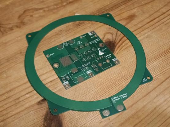
Here we go, a Revision 2 of the board! I think it's ready to send to the fab, but inevitably I'm gonna find some small things to tweak after posting.
Light blue rectangle is the outline of a big heatsink on the back side of the board.
Thanks to @gsuberland and @electronic_eel for their input on thermals :)
new boards already arrived!
ngl I'm a bit spooked by how fast and I
inexpensive it was, even though there's pretty explicitly some kind of promotional/loss-leader pricing going on.
Also these are 0.8mm boards (half of "standard" thickness) which should help with both front-back thermal conductivity and make the two-layer inductor a little more inductor -y.
oh yeah, seen in action here is a hot tip I'm only recently internalizing:
if you're making a thing and it has screw and/or mounting holes, mark the screw size/spacing directly on the object if at all possible.
it is with profound excitement that I'm able to finally unshroud the project I've been working on:
xenon plasma toroid
(also I had to duck the volume in this clip because my "let's gooo" was too loud)
tried to run the toroid off of my beefier bench supply and blew a mosfet.
It's looking like the driver is probably drawing a lot more current than simulated. The miniware psu (and the USB-PD supply) I used yesterday handles brownout pretty gracefully, but I suspect the bargain bin bench PSU is less graceful.
Part of the higher power draw could be due to messy switching, but if I lower the primary cap values in the sim to 66pF (from the nominal 99pF) I get results more similar to the observed circuit. I don't think the frequency or temperature is high enough to cause that kind of de-rating but who knows, could be as simple as one of the three capacitors has failed.
Going to order some more caps, this time explicitly marked as low-ESL.
Still not sure what's up with the coil getting blazing hot.
Good news is, @x44203 was totally right about the apparent higher-frequency jigglyness of the mosfet gate trace being due to my scope probe having too long a ground lead. Using the spring-probe shows much cleaner waveform!
still not the clean sine-wave I'm hoping for, but better.
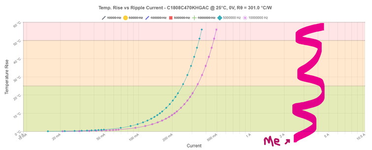
...not the exact capacitors I have installed, but similar.
Using a bank of only three is *definitely* asking too much, even if I think things aren't quite as bad as 300°C/W. Note the log scale on x-axis.
Sincerely though, does anycritter have ideas on why the two-turn 1.9uH PCB coil gets so dang hot?
According to the saturnPCB calculator / IPC 2152, I'd expect less than 30°C rise to steady-state even taking skin effect into consideration, based on my ltspcie sims expecting ~12 peak amps at ~13MHz (sinusoidal).
I see like 70°+ temperature rise within a minute.
Guessing there's something going on with inductor energy getting dumped as heat, so resistive load calcs go out the window. But I have no idea how to reason about those possible effects.
...I suppose the board is taking like 40W input so clearly the power needs to go *somewhere*. I was hoping that most of the somewhere would either be making the xenon get all bright, or else drifting away as legally iffy radio.
lol so ended up just using I^2 *R just given DC resistance of a few tenths of a ohm and amperages in the 6-10A range...
that's multiple tens of watts of heat.
Very rough estimates of thermal mass give many degrees per second rise.
...yep there's a problem.
So the standard trace width calculations just aren't remotely applicable here apparently!
I now slightly better understand why other folks haven't used PCB inductors here.
I suspect I might still be able to donut with much lower amperages though! If I get down below 3A in the inductor, that's only like four watts heat rather than dozens.
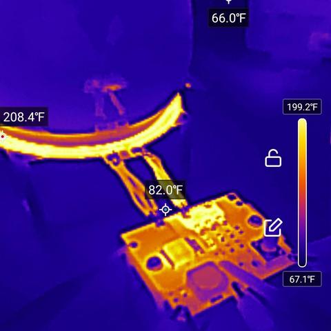
Here's a li'l gif of my inductor coil trying very hard to burn itself to a crisp. Spot-point temperatures come on-screen near the end.
~130°C in about 30 seconds.
writeup updated
https://hackaday.io/project/194683-plasma-toroid-sky-guided-pcb-edition/log/227533-i-would-like-my-circuit-to-not-cook-itself
https://hackaday.io/project/194683-plasma-toroid-sky-guided-pcb-edition/log/227533-i-would-like-my-circuit-to-not-cook-itself
i would like my circuit to not cook itself | Details | Hackaday.io
<p>First Light accomplished. What did I learn?<br><br>The circuit in its current iteration,<br>1: gets hot alarmingly quickly<br>2: is trying to draw more power than I can actually supply. <br><br>Those seem related, yeah. <br></p><figure><img data-src="https://cdn.hackaday.io/images/6280501708053920075.jpg" class="lazy"></figure><p><em>apologies for the excessively american temperature units<br></em><br></p><p>Based on simulating the circuit in the condition tested, at 15 volts supply I'd expect to see something like 50W power draw, at around 3.5A. The tests discussed in the previous post sure looked like the USB-based bench supply was badly voltage sagging, so the next day I hooked up the beefier bench supply -- and very quickly started sagging, then blew another mosfet. I <em>suspect</em> that this very-budget bench supply has some sort of destructively un-graceful switch from constant-voltage to the constant-current mode it failovers to when it hits 5A, but it's also entirely possible that the mosfet blew first and I saw the power supply feeding a shorted chip. <br><br>My power budget is <5A @20V (the 100-watt maximum of USB-C-PD), but I'd prefer to stay <60W if possible.<br><br>If I simulate a lower primary capacitance (e.g. 66pF instead of the as-built 99pF), power draw is dramatically greater <em>and</em> the higher resonating frequency is also a closer match to what I observed on the
More progress on the plasma toroid! More videos! Less overheating!!
Writeup at https://hackaday.io/project/194683-plasma-toroid-sky-guided-pcb-edition/log/227790-tweakin
Higher-quality vid at https://www.youtube.com/watch?v=rEc76ckTJcg
tweakin' | Details | Hackaday.io
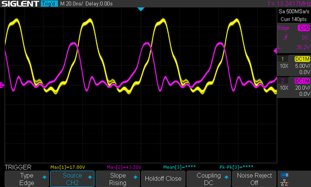
<p>Spent a big chunk of the weekend adjusting a variety of component values. <br></p> <figure><img class="lazy" data-src="https://cdn.hackaday.io/images/7189551708888806047.png"><br>Here's the waveforms with the circuit unloaded (no toroid), at 18V supply:<span></span></figure> <figure><img class="lazy" data-src="https://cdn.hackaday.io/images/2465921708889099062.png"></figure> <p>Yellow is Gate (5V/div), purple is Drain (50V/div), blue is feedback network bias input at TP5 (5V/div).</p> <p>Looks decently healthy to me. I suspect that the gate protection zener diode is doing its job and helping to keep drive voltages within operational limits.<br><br>Here's the traces when the xenon is fully toroid-ing:</p> <figure><img class="lazy" data-src="https://cdn.hackaday.io/images/1735241708891968601.png"></figure> <p>Hm. Clearly the device is overall functional but these waveforms aren't as clean as I'd prefer. Maybe it's fine?</p> <p><br>All right, so let's walk through the component changes. I'll spare the step-by-step of each individual test -- most of it was poorly documented and I was going for more of a "better or worse?" approach than robust characterization. <br><br>First off, primary tank capacitance was increased 99pF to 141pF. This was the first change made, as planned in previous project log "<a href="https://hackaday.io/project/194683-plasma-toroid-sky-guided-pcb-edition/log/227533-i-would-like-my-circuit-to-not-cook-itself" target="_blank">i would like my circuit to not cook myself</a>". <br><br>Increasing capacitor value was broadly successful -- overall power draw was reduced to ~2.9 - 3.2A depending on circuit configuration. Yay!<br><br>Decoupling cap C4 was removed because it caused some kind of runaway oscillation on
More plasma toroid progress! Things are going super well!
Video demo:
https://youtu.be/fBrOaj5pBa0

Plasma Toroid WIP demo #3 - ✨😇
I'm at a point where I could call this "done" if I wanted.
It's not done yet though ^_^
roflll, I'd been working hard to implement a subcircuit for monitoring current draw to indicate out whether or not the primary inductor was in oscillation, using a shunt resistor + op-amp + comparator etc.
And just now realized I can do the same thing *better* using nothing but a loop of wire and an LED.
technically I do also need a current limiting resistor. Burned out my first LED.
ofc this'll be turned in to a loop trace on a circuitboard soon enough, rather than a test lead wrapped into a spiral.
Feeling *very* pleased with myself right now.
Plasma toroid project writeup has been updated, with details of the non-contact indicator light shown in the previous video clip.
"status LED, galaxy brain style"
https://hackaday.io/project/194683-plasma-toroid-sky-guided-pcb-edition/log/228373

status LED, galaxy brain style | Details | Hackaday.io
<p>Since a key goal of this project is to run standalone -- no o-scope, no bench PSU, no amperage panel meter -- it's crucial to have some sort of indication of whether the circuit was in oscillation or just sitting idle.<br></p> <p>Overall power draw reliably reflects the circuit's state. When not oscillating, there's near zero draw -- just LEDs, leakages, etc. While running the draw is more like 2-3 amps, and can be reduced down to as little as ~1.2A by lowering mosfet gate bias. </p> <h1>The normal approach</h1> <p>I had initially planned to use the pretty typical current monitoring method of a differential op-amp measuring voltage across a low value shunt resistor. Since I'm looking for a threshold current indicator rather than a continuous analog signal, the op-amp is fed into a comparator, against a reference voltage.<br></p> <figure><img class="lazy" data-src="https://cdn.hackaday.io/images/3954551711072740439.png"></figure> <p><em>Yes, this diagram is kind of sloppy, but you won't need to linger on details here anyway. If the text is unreadable due to aliasing you can click to embiggen.</em></p> <p>The TSM102 IC seemed like a neat combo-wombo of packaging two comparators, two op-amps, and a 2.5V reference all in one. It's also relatively inexpensive and can run off of a 40V Vcc. Purpose-built current monitor
ANOTHER plasma toroid project update: Pushbutton Arc Start!
https://hackaday.io/project/194683
This one is a big deal, since I've now hit every core functional milestone. The next steps are putting all of the subsystems together into a single, unified board.
This subcircuit is also neat because it uses multiple different bits of antiquated technology: photo-flash trigger circuits and gas discharge tube surge arrestors.
(demo vid attached here; high-quality available on youtube https://youtu.be/Vi6Pb0WSCZw )

Plasma Toroid (sky-guided PCB edition)
status: v0.1 failure (mosfets destroyed: 5) v0.2 success v0.3 better performance Mission: Create an inductively coupled plasma toroid in a globe of xenon gas. The end goal is to have all electronics (including primary inductor) part of a single PCB running on USB-C-PD power, in a well-built and aesthetically attractive presentation. Inspired by "perfecting and explaining the plasma toroid" by BacMacSci https://www.youtube.com/watch?v=GbMAvn7nRWo The driving electronics is a "class E" self-oscillating circuit based on a SiC MOSFET. A ~2µH loop inductor is driven at 10-15MHz and >2kV, creating a strong electromagnetic field. If a 1-liter globe of ~15 torr xenon is placed in the middle of the inductor, the xenon will ionize into a conductive loop analogous to the secondary winding of a transformer. based on the work of Steve Ward and BacMacSci.
@skyguided holy shit so badass !
@skyguided If your PCB inductor is still getting too hot, if you put some large through holes on the solder pads for the wires, you could just stack a bunch of those PCBs right on top of each other, connect them at the pads and get more copper and more surface area for skin effect.
@skyguided I can imagine that maybe part of why you get so much heat (besides the I^2*R thing) might be that the skin depth is only negligible at your nominal frequency, but is significantly lower for higher-frequency components, especially if you still have a couple watts going out at 100MHz from some parasitic oscillation.
@skyguided Purely incidental, something I've found designing a similar resonant thing was that many high-capacity (tens to hundres of nF) MLCCs perform poorly at high-ish frequencies, and film caps perform much better at a comparable price point. They are much larger though.
@jaseg the primary inductor current *should* be quite sinusoidal, but that's a line of inquiry with looking into, hnlm 🤔
@skyguided hell yeah hell yeah! lookin sick c:
@skyguided Good write-up, I'm enjoying seeing the development process of this project!
@skyguided this is so fucking cool 🤩

@skyguided yeah, probably best to use real thick copper
or possibly a formed coil made of copper tubing or litz wire instead of a pcb coil
-F
@skyguided Are you certain it's 12 A peak? are you certain it's 1.9 μH?
-F
-F
@Hearth I have no obvious way of probing the amperage so I'm basing that off LTspice
1.9uH was based on measuring resonance against a 10nF parallel cap -- hitting the coil with a square wave and measuring the period of the resultant ringing.
@skyguided Probing the current would most cheaply be done with a current transformer--but ones of those good to multiple megahertz are still a few hundred bucks so possibly out of reach unless you have a contact with one handy (ask about Pearson transformers--look at their catalog to see what specific ones would work)
When you measured the inductance, what were the surroundings? Are they the same as the current surroundings? Any magnetic or conductive material nearby can mess things up
-F
@Hearth inductance was measured sitting on a wooden tabletop, with the middle aperture empty. In the real circuit it's 50mm off the tabletop with a bit of glass and some near-vacuum xenon in the center. I figure those kinds of difference are well under measurement error.
@skyguided OH i realized the problem
your whole point is to transformer-couple eddy currents into the xenon globe
that's a conductive plasma ring that acts like a shorted turn on the poorly-coupled transformer consisting of the pcb inductor and the plasma loop
that will drastically reduce the effective inductance in practice, so your currents may be many times higher than what you calculated
-F
@skyguided we are going to get dinner now but will think on if we have any tips and get to you later--the best tip we have right now might just be to make the inductor able to handle more current by using 2 or 3 oz copper and wider traces
-F
-F
@skyguided (also calculating the new effective inductance would be a very complicated matter because the shape of the plasma ring and the degree of coupling to it would be pretty variable and hard to predict)
-F
-F
@skyguided (also also plasma conductivity is highly nonlinear so that's another layer of complication in the mix--basically trying to calculate it is likely futile)
-F
-F
@Hearth the inductor does get real hot even when unloaded, but spitballing a transformer secondary in LTspice definitely does completely mangle my previous simulation results.
@skyguided 12 A is still a lot of current to be putting through PCB traces. I expect the current is significantly higher once the plasma forms, though, so it'll heat up much more with it than without.
-F
-F
@skyguided its likely coming from the "Proximity Effect" which is kind of generalization of the "Skin Effect"
Current in one trace tends to push away current in neighbouring traces, so the current might flow in less than 1mm width of a 10mm wide trace
The best thing you could do at these frequencies would be a ring of copper foil rotatet 90° to be paralell
The second best is a coil of smooth and preferably silvered wire or tube, to have most possible surface area
Litz works not so well here
@skyguided if you might happen to be around europe, expically germany, i would be happy to help you building a better inductor
Also, do you have a good image of your control board, please? I would be happy to check if i see ideas to improve it
@skyguided If you can fit it, 2220 is a good package to use for this kind of high-voltage stuff
plenty wide for comparatively low inductance, and Big so it can handle a lot of power
-F
@Hearth Based on the Kemet sim tool, impedance (as a function of frequency) and temperature rise aren't dramatically different between 2220 and the 1808's I'm currently using. I think I just need to share the load between more of 'em.
@skyguided That'll work too, yeah. One of the advantages of 2220 is just that you're spreading the power dissipation over a larger area, though, so they'll stay cooler
That also can be done by using more 1808s though
-F
@skyguided If not for the voltage requirement, I'd also suggest reverse terminal packages like 0508--having the terminals on the long side reduces ESL by quite a lot actually
but of course that puts the terminals closer to each other which is not really practical if you want kilovolt ratings
-F
@skyguided (and silicon capacitors get remarkably low ESL--in the tens of pH--but they are typically only rated to like 25 or 30 V)
-F
-F