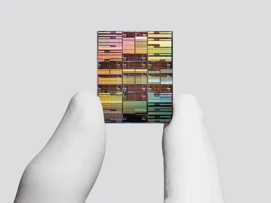
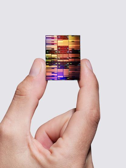
IBM ha svelato il primo chip a 0,7 nanometri, utilizzando l'architettura #nanostack per portare i nanosheet in 3D. Un passo avanti significativo per l'industria dei #semiconductor e della #tecnologia.

My roundup of this week's big #AI infrastructure news from #Qualcomm #OpenAI / #Broadcom and #IBM is below. The common thread? Tackling AI's cost and energy efficiency problems. #jalapeno #nanostack
Read it here: https://www.techtarget.com/searchitoperations/news/366645030/Qualcomm-OpenAI-IBM-target-AI-infrastructure-efficiency
IBM Claims To Have Created World’s First Sub 1nm Chip #hardware #ibm #nanostack #semiconductorchips #sub1nm
https://www.lowyat.net/2026/396948/ibm-claims-to-have-created-worlds-first-sub-1nm-chip/
FinFET, Nanosheet, Nanostack... learning new things every day!
That said, I think it’ll take a few more years before we see these breakthroughs in commercial AI chips.
Therefore, we're likely to see the AI bubble pop. Soon. Then, once time has passed, we’ll finally benefit from cheap AI utility services as human productivity accelerators.
🚨 NEWS: IBM presenta un chip sub-1 nanometro con nanostack che raddoppia la densità dei transistor
Ecco i punti chiave in breve:
💡 IBM ha svelato un prototipo di chip con circa 100 miliardi di transistor su un'area grande quanto un'unghia. Questa architettura, chiamata nanostack, impila verticalmente i transis...

🚨 NEWS: IBM svela chip sub-1 nanometro con architettura nanostack per data center AI
Ecco i punti chiave in breve:
💡 IBM ha annunciato una nuova architettura di chip che integra quasi 100 miliardi di transistor su una superficie grande quanto un'unghia, raddoppiando la densità rispetto alla gener...

IBM hails new 'block of flats' design breakthrough for tiny chips
IBM says it has created the world's first known chip tech below 1 nanometre - but it will be some time before it's ready for production.


Today IBM is unveiling their nanostack transistor architecture. Meant to drive chip construction in the sub-1nm era in the 2030s, nanostack aims for building better and smaller chips by building them taller via wafer stacking