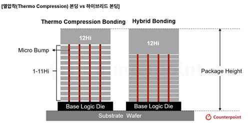
Hybrid bonders are all the rage at fabs around the world that produce high-bandwidth memory & AI chips.
The world leader in hybrid bonding is a 🇳🇱 company called Besi.
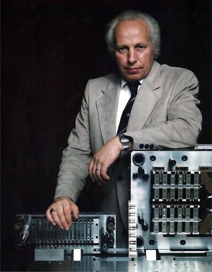
Today, we pay tribute to Richard Fierkens who passed away on Sunday. He founded Fico Toolings, laying the groundwork for Besi.
Fico started in 1956 from a workshop in Herwen, producing molds for simple plastic products such as coat hangers and milk crates.
https://bits-chips.com/article/richard-fierkens-1935-2026-a-forgotten-dutch-chip-pioneer/