Finally starting to dust *this* board off.
I think it's been a while...

Security and open source at the hardware/software interface. Embedded sec @ IOActive. Lead dev of ngscopeclient/libscopehal. GHz probe designer. Open source networking hardware. "So others may live"
Toots searchable on tootfinder.
| ngscopeclient | https://www.ngscopeclient.org/ |
| Blog | https://serd.es |
| Location | Seattle area |
| GitHub | https://github.com/azonenberg |
Found the first bug before even starting the SI simulations I had planned to be running.
SFP28_0_TX is missing the ground plane voids under the BGA lands.
But before I add them back it'll be a good excuse to simulate both launches and see how much a difference it really makes.
@dlharmon The specific techniques I am playing with improving right now are wire bonded, overmolded BGAs with organic multilayer substrates which are somethign I encounter decently often and have never been thrilled at QoR in my home lab.
At work we use fuming nitric which cuts through the BT like butter and you just get clean sheets of resin-free glass mesh floating in the acid lol.
@dlharmon Well, I can still image the chunks if that is in fact the case.
I still have a few of the other parts you sent me like the 7k70t FBG484 that are in the queue and not yet touched.
For those, I'm wondering if a more standard chemical decap might be fine to eat the underfill and edge bond, then either switch to dilute acid or heat to melt or etch off the solder bumps. I'll need to experiment a bit.
@dlharmon Once you finish the reballing tests if you send me the intact chip I wanted to test some higher end techniques on the mill for better-planarity substrate delayering. I can also do really high res imaging of each layer.
Of course, if you want to try your hand at it, that's fine too
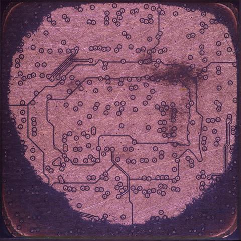
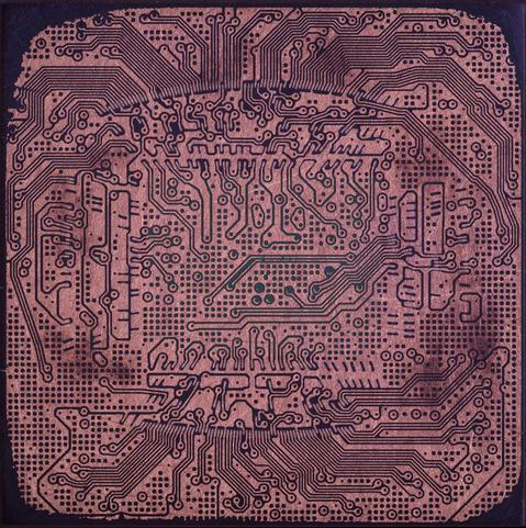
Metal 1, coming up on the underside of the die. You can see all of the little wire bond rings, 4-5 concentric rings of wire bonds.
I sanded up to the silver epoxy but not into the silicon to avoid potentially cracking it. So we should get a really clean die back side at the end of this.
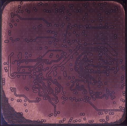
Metal 2.
This turned out really good, planarity actually *improved* as I got deeper which surprised me because usually it's the opposite. Not sure if I was getting the feel of the part and correcting as I saw unevenness, or something about the way it was flexing, or what. But it seems like there is less edge rounding now.
There's a few obvious thicker zone fills, maybe power tracks? And a lot of signal routes, including some length-matched diff pairs.
Most of this layer is one big zone fill that I suspect is ground but have not probed to confirm.
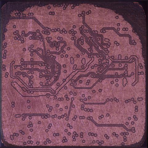
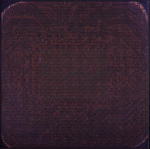
Metal 3. Lost a bit of the edges especially along the south side but got most of it (and you can see some of the missing parts in the previous image).
Looks like mostly power rails, likely VCCO / VCCINT / VCCAUX although I haven't mapped out which is which yet. Possibly some ground too. And a few IOs in oddball places.