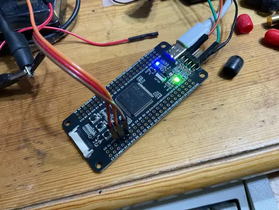
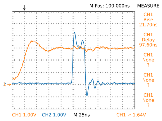
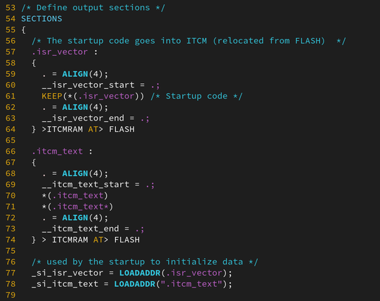
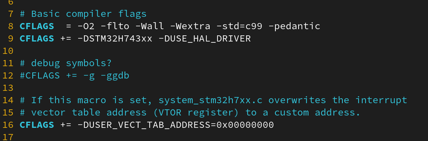
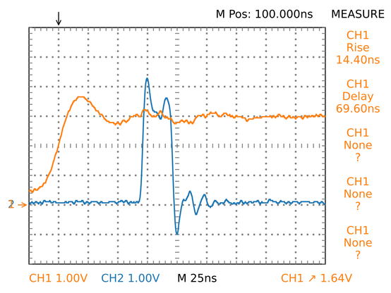
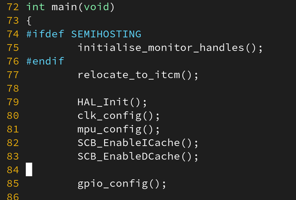
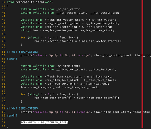
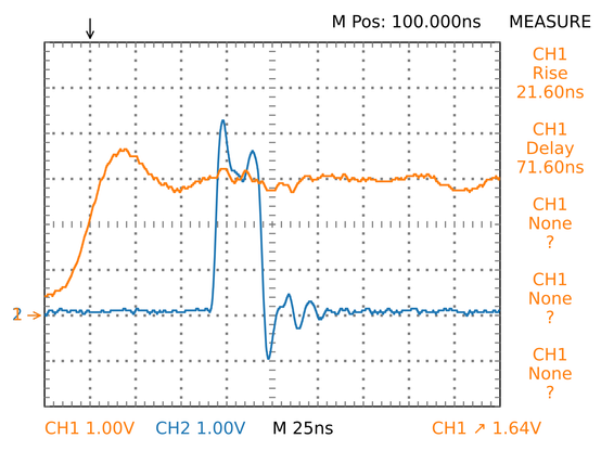
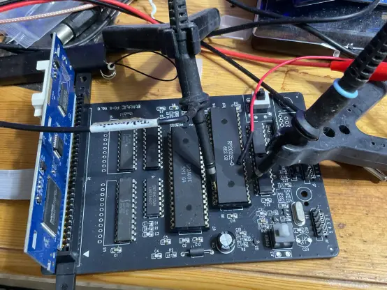
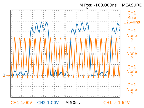
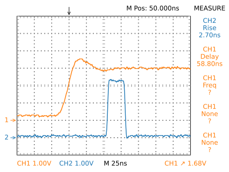
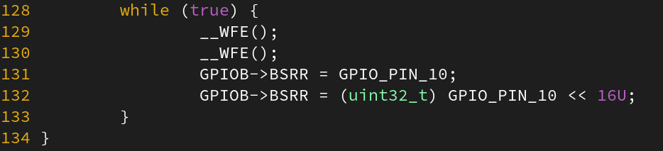
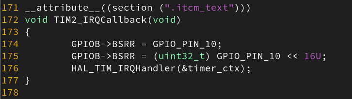
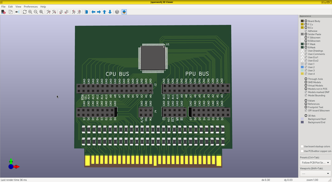
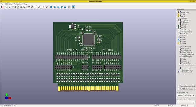
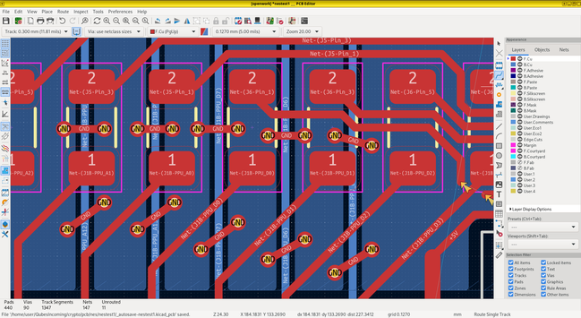
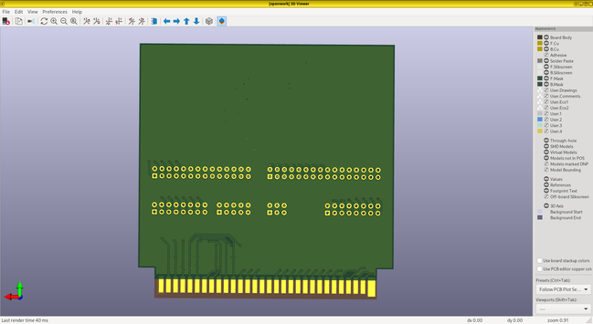
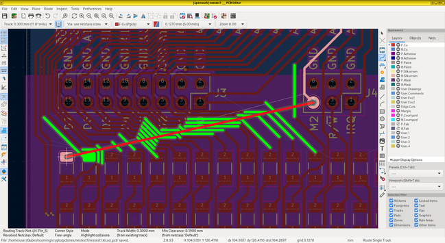
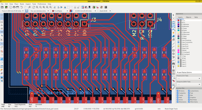
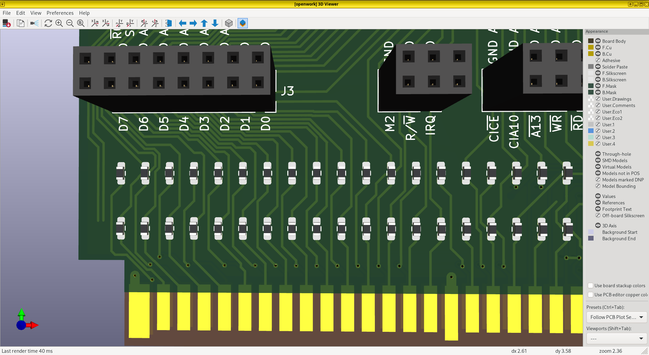
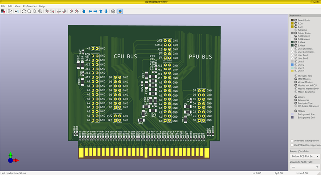
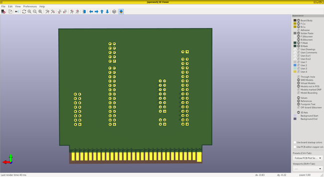
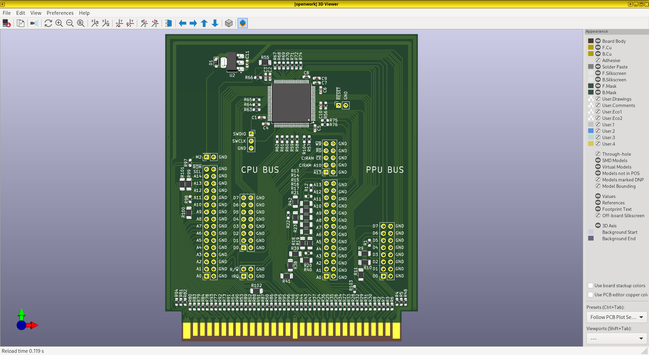
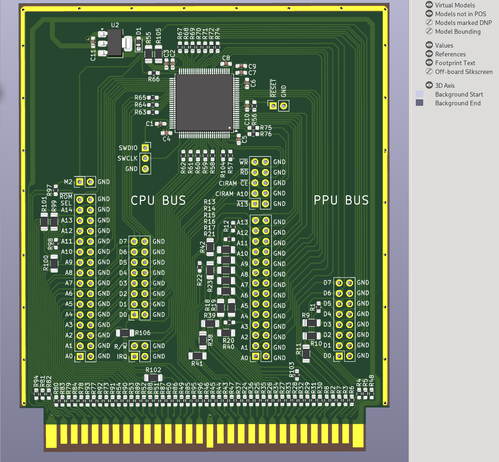
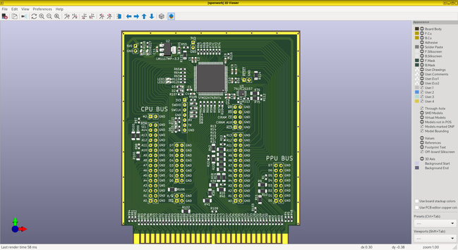
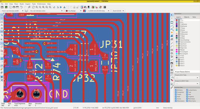
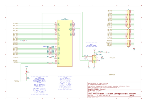
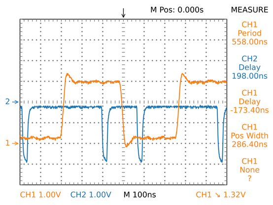
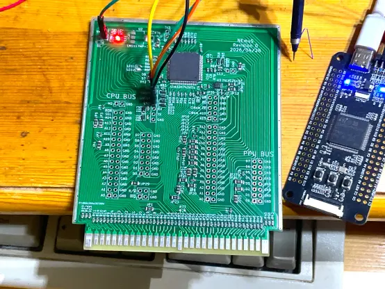
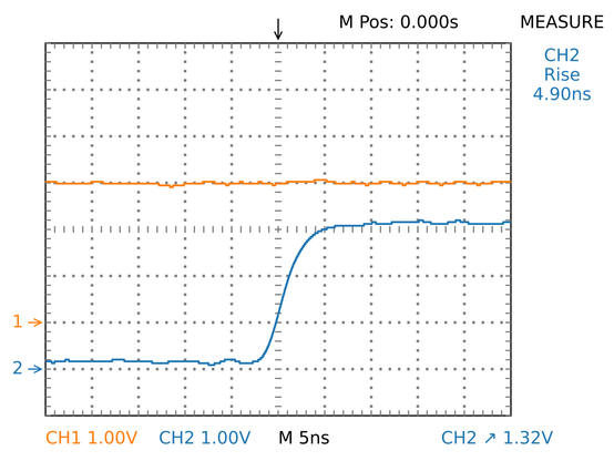
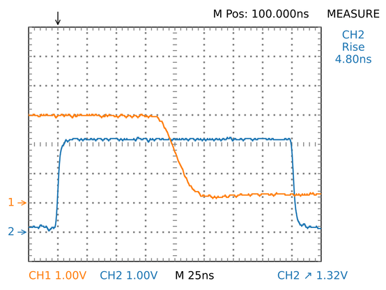
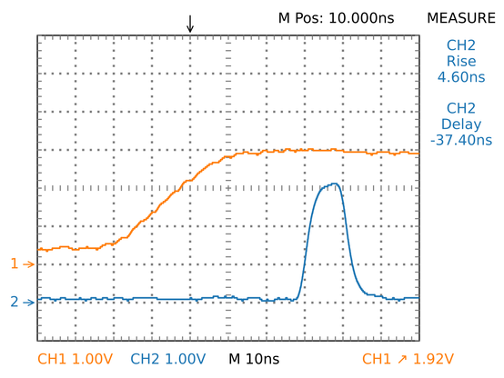
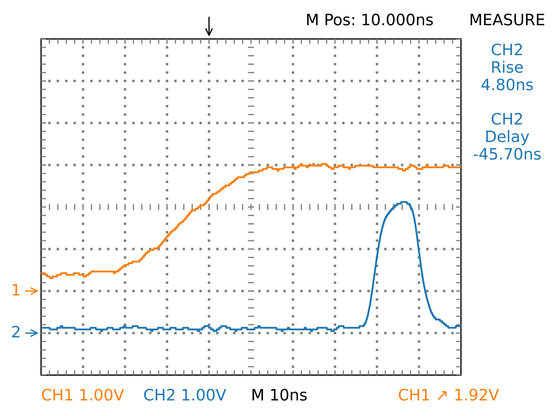
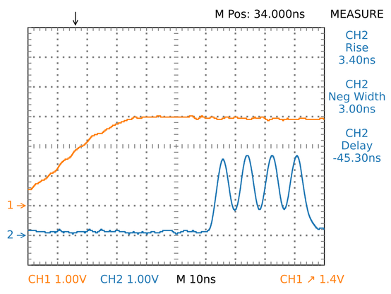
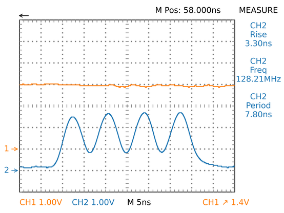
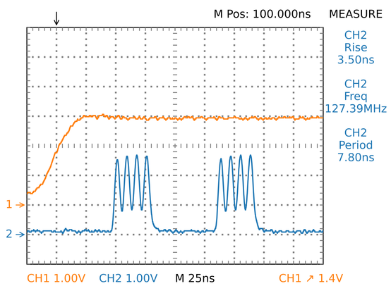
Optimizing IRQ latency on the STM32H743 @ 480 MHz, perhaps for NES ROM emulation... Best result so far: 100 nanoseconds input-to-output latency when the vector table and the IRQ handler are relocated to Tightly-Coupled Memory without making HAL calls. Not bad, but the GPIO controller (several buses away) looks like the real performance killer here. WARNING: buggy code, see correction https://mk.absturztau.be/notes/ajvb448y305b01i4. #electronics #STM32
Keep optimizing IRQ latency on the STM32H743 @ 480 MHz. Just enabled i-cache and d-cache, and the IRQ latency dropped from 100 ns to 70 ns. 🚀 But cache shouldn't work like this. So my code is still touching slow memory somewhere. The stack perhaps, which is still in "normal" RAM. The slow Flash perhaps also makes it slower to abort main() if an instruction is stuck in a wait state. Need to check everything carefully... #electronics #STM32
Keep optimizing IRQ latency on the STM32H743 @ 480 MHz. The 70 ns vs. 100 ns overhead mystery solved. I did not correctly relocate the vector table to Tightly-Coupled Memory properly, it was still in Flash. The STM32 HAL macro USER_VECT_TAB_ADDRESS is a flag, not a memory address! In fact, only several hardcoded addresses are available, a real user override is not provided (the name "user" is a lie). Solution: just change VTOR manually, don't trust the startup code. I'm now getting 70-ns IRQ without CPU cache. #electronics #STM32
I do not understand how the NES system bus works, even after reading multiple tutorials. Only one way to find out... #electronics #NES #NESdev
Keep optimizing IRQ latency on the STM32H743 @ 480 MHz. I decided to try an event loop using the WFE instruction instead of IRQs, and I managed to get 60 ns input-to-output latency. I suspect this is the best possible latency. Latency did not improve by abusing QSPI controller to generate a write request (in fact it slightly degraded), even if the QSPI controller is physically close to the CPU. Clearly, passively monitoring signals is not the way to go for bus emulation. Perhaps the solution is predicting the clock before it even arrives, by internally generating a phase-shifted version of it. #electronics #STM32
Keep optimizing IRQ latency on the STM32H743 @ 480 MHz. My "zero-latency IRQ" idea is a success, now I'm getting a 17.30 ns "effective" latency! Upon receiving every rising edge of the clock, the hardware immediately starts a timer that fires after a programmed delay, calculated to be slightly before the next clock rising edge. This way, the firmware is triggered from recovered, phase-shifted version of the clock, a little bit like how analog NTSC TVs got their H/VSYNC. Interrupt latency is completely eliminated for all but the first clock cycle (which is also predictable with pre-enabled outputs, since it's always the reset vector) Perfect bus emulation starts looking feasible. #electronics #STM32
Making a 60-pin Famicom debug cartridge for testing my cartridge emulator... #electronics #NES #NESdev

"Warn : no flash bank found for address 0x08100000"Spent half an hour trying to figure out why can't OpenOCD see my upper flash bank, while claiming my STM32 is dual-banked at the same time. Solution: use stm32h7x_dual_bank.cfg, not stm32h7x.cfg. ​#electronics #STM32

Still working on the same 60-pin Famicom cartridge emulator devboard. Finding a single-layer solution for the 480 MHz STM32H7 on a 2-layer power+signal / GND only stackup is like kicking a dead whale down the beach. I should've used a 4-layer board, but at least I now have the bragging right of developing the least radiative 2-layer PCB for the NES. #electronics #NES #NESdev
Still working on the same 60-pin Famicom cartridge emulator devboard. #electronics #NES #NESdev
EMC Pro Tip: rejoin the GND later nearby if you must split it, so the loop area doesn't go off the chart. P.S: I think a ground pour with vias should work even better here, as the signal traces would form coplanar waveguides with well-defined reference planes on the same layer. #electronics #NES #NESdev
The holy grail of 2-layer PCB is when you have just a metal sheet on layer 2. I think I'm quite close, but unfortunately some external jumpers are needed to finish the remaining control lines without cutting this beautiful plane. Even THT resistor jumpers are not enough to jump across the 24-trace bus. #electronics #NES #NESdev
NES quirk: the VRAM has two memory layouts that "wraps back" either horizontally or vertically for different scrolling games. This is called "nametable mirroring" mode, controlled by routing the raw "CIRAM A10" signal to the PPU A10/A11 address line via the cartridge port. But for my cartridge emulator, it means we're not just acting as a device sitting on the bus, it's actively messing with the PPU bus on the whole machine. Do I have enough time to do it in software GPIO, or do I have to use an external 2:1 hardware mux? Let's see:

* Hitachi HM6116 - Read: address valid prior to or coincident with /CS low. Write: address setup time 20 ns.
* Panasonic MN4216 - Read: address valid prior to or coincident with /CS low. Write: address setup time 20 ns.
* Sony CXK5816PN: Write: address setup time 0 ns.
* Sanyo LC3517: Write: address setup time 0 ns.

Conclusion: don't worry about it, "copy an address bus line 20 ns before /CS falls" is not a significant timing constraint to the existing 180 ns budget for the emulator.
#electronics #NES #NESdev
Downsized all input resistors from 1206 to 0603, preparing to use the extra space for more air bridges. I initially switched from 0603 to 1206 to give space for horizontal traces, but I found it did not really have any advantage in comparison to 0603, as the vertical traces blocked all the horizontal ways anyway, 0603 + selective 1206 jumpers probably can solve this deadlock. #electronics #NES #NESdev
Unfortunately the original layout couldn't be completed because the placement and fan-out were not designed with "single-layer flowthrough" in mind, as I originally had no idea about the pinout. The whole board layout was thus abandoned and restarted. Now I have a 99% zero-gap ground plane, with only 13 non-perpendicular cuts under the connectors without interrupting GND. An army of 0-ohm jumpers bridge signals to human-friendly positions. #electronics #NES #NESdev
Almost finished my Famicom cartridge devboard. This time all signals fanned out successfully under the 2-layer + "Zero Gap" ground plane constraints. 100 MHz signal integrity disciplines applied to a 1 MHz bus. #electronics #NES #NESdev
devboard 100% routed. #electronics #NES #NESdev
I've killed way too many STM32s in my early life. You basically just program the target as usual, but after power cycling it several times, suddenly every GPIO is shorted to GND. Likely current injection, latch-up, or both. So this time let's try not to kill it again. At the SWD port, 1 kΩ + BAS54 clamps voltage and current to VDD + 0.4 V and 3.3 mA respectively. #electronics
Murphy's law again: STM32 has many 5 V tolerant pins, except the pin you're going to use. #electronics
@niconiconi STM32 are nasty micros. Along with PICs. Do not want.
@ozeng @niconiconi oh from my usage they're less nasty than PICs by orders of magnitude!
Fixed more problems found in design reviews, such as connecting 5 V inputs to some 3.3 V-only pin. There's also no time to generate the /CE signal for PPU VRAM, unless the microcontroller itself emulates the VRAM. This is too much effort to implement for the first phase development, better to use an external mux for now. #electronics #NES #NESdev
ProTip: You can pretend to be both an old-school engineer and an RF engineer by enabling "fillet tracks" ​#electronics #NES #NESdev
Trying to keep my schematics as readable as possible, as usual. #electronics #NES #NESdev
#STM32 timer trap for young players: Channel 3/4 have input edge detectors, but their outputs TI3FP3 and TI4FP4 are NOT physically connected to the trigger controller! ​​ You can only trigger from Channel 1/2's TI1FP1 and TI2FP2. But if you only need one input channel, there's a way to save it: enable the XOR gate meant for Hall sensors, and set unused Channel 1/2 to 0 via forced output mode (no need to attach them to actual GPIOs). #electronics
Unbelievable. I wanted to simulate the NES CPU clock so I turned the knob on my analog function generator (no DDS/PLL, with digital counter) for 1.79 MHz randomly. After running it for a day, I found the oscilloscope shows the signal has a period of 558 ns (the theoretical period should be 558.73 ns). Nanosecond precision with a potentiometer. ​#electronics #NES #NESdev
My Famicom cartridge emulator devboard arrived, time to start developing firmware using this platform. #electronics #NES #NESdev
My RF design rules paid off! The 5 ns edge from the STM32H7 GPIO is one of the purest edges I've ever seen, even though I'm using a two-layer board (which features 120 Ω all-microstrip routing on a gapless plane, source termination, and one ground per signal test point). It's even cleaner than my clip-connected function generator. #electronics #NES #NESdev
The decision to connect GPIOs in random orders for PCB layout optimizations might be a mistake. I suddenly need to deal with this man-made horror beyond my comprehension. #electronics #NES #NESdev
Keep optimizing and benchmarking the IRQ latency of the STM32H743 @ 480 MHz. Ultimately, I was able to achieve a WFE polling latency of 38 ns, and an IRQ latency of 45 ns. I think these numbers are close to the theoretical limits. Source code on Codeberg.

The slow AHB bus and the GPIO controller prevented me from measuring the true IRQ latency of the core itself accurately. But I found a way out: EVENTOUT. Inside the ARM IP core, there's an internal signal called TXEV, originally meant for synchronizing multicore systems (by connecting it to the
RXEV input of another core). On the STM32, TXEV can be mapped to any GPIO pin, allowing single-cycle pulse generation directly from the core via the SEV instruction without any controller overhead. #electronics #STM32
Keep optimizing and benchmarking the GPIO latency of the STM32H743 @ 480 MHz. I can now generate a pulse width below 3.9 ns, or a pulse train over 127 MHz! At a latency of 45 ns.

I was able to break the GPIO's 20 ns width barrier using DMA1. The BDMA in theory has the best memory locality in domain D3, but it's slow. Meanwhile, domain D2's DMA1 has a FIFO and supports AHB burst transactions, dramatically reducing the latency per toggle within a burst. I think this is the fastest pure GPIO bitbanging method on the STM32H7 using the actual GPIO controller. This shows the raw GPIO controller is fairly fast, it's just challenging to feed data into it.

See
ST forum thread and EEVblog thread for details. #electronics #STM32
Trying to change the DMA registers within the DMA itself, so I can create a new DMA write based on the previous DMA read. It's DMAception. Not sure if it works, still need testing. #electronics #STM32
Blinking a LED using STM32 DMA — whitequark's lab notebook

@r The STM32H7 has a new "MDMA" engine with chaining support, explicitly designing for gather-scatter. I'm trying to master the conventional DMA first (as described in the blog post).
@niconiconi I wanted to do this with an 8259, but determined I would have to use 2 of them
@niconiconi The last one looks like Groke's hands. Scary stuff.
@niconiconi omg, so many times I have wanted exactly this! Thank you for posting about it
@niconiconi the cited taocp section has a clearer explanation of how this works i think
@niconiconi It resembles an Enigma machine
@s_wilson Indeed, there are many papers on optimizing the bit-permutation steps of hardware crypto accelerators using these networks.
Dang that is clean, @niconiconi.
@niconiconi That's awesome, the NES won't gonna believe how clean that is!
@doragasu Still going to have some reflections at the uncontrolled edge connector with only two GND pins, but that would be someone else's problem.
@niconiconi Well, it's a NES after all, I suppose it doesn't need to run at 5 GHz 😁
@niconiconi How did you create that screenshot?
@tom_verbeure I have a custom script that calls almost every command available on my Tektronix TDS200 series oscilloscope to "save state" as a JSON file. This JSON state is fed into a custom Python matplotlib script to draw an oscilloscope screen grid by grid in a style similar to the real UI, then it generates an SVG. This SVG is then rasterized to a 300 DPI PNG.
@tom_verbeure This is what the raw data looks like, which is rendered as a publication-quality plot. I never shared the script because everything is tied to the TDS 200 and I don't have the patience to make it extensible. But perhaps the oscilloscope screen drawing code is of some use.
@niconiconi @tom_verbeure ohhh, I'd love to see the screen drawing code
@whitequark @tom_verbeure It's basically the Python equivalent of vacuum tube electronics. Took no brain to write (with hardcoded coordinates, arrows, sample length, etc), but a lot of patience, and there's still no support for non-waveform features like FFT which would require repeating the same grind. A proper front-end or graphics should be able to do it much better.
@niconiconi @tom_verbeure yeah tbh I'd reuse that. if I want SVGs to embed into docs that's totally serviceable as-is
tdssave

Saving raw oscilloscope measurements and states, and plotting them as vector images. Hardcoded for the Tektronix TBS1102 oscilloscope (similar to the Tektronix TBS200 series oscilloscopes from the early 2000s).

Codeberg.org

@niconiconi I like the old school look for my blog posts and went out of my way to get it, but this really looks great and it should work with my TDS220.

https://tomverbeure.github.io/2024/11/29/Making-Screenshots-of-Test-Equipment.html

Making Screenshots of Test Equipment Old and New

Electronics etc…
@tom_verbeure You may need to tweak the code somewhat, as the register definitions of my TBS1100 series (which is a rehash of the TBS200) are slightly different.
@niconiconi We need a photo of the analog function generator
@anachrocomputer Generic IC-based function generator from the early 2000s, with a "Civil Aviation University of China" asset tag. The range switches and counters are digital, but the pot is analog.
Actually Useful Schematics (in KiCAD!) (KiConn 2025)

Useful Schematics Or, “Don’t make me want to murder you” Andrew Greenberg Senior Instructor, Portland State University [email protected]

Google Docs
@mdc No, I've never seen this presentation. But I did see the 1970s Tektronix schematics which were cited in this presentation as well. Those schematics are always my personal benchmark of "good schematics", just like the author. I guess it's what Abel said, "one should study the masters and not their pupils." I learned that from the primary source.
@niconiconi it bothers me that D7-D14 are not vertically aligned in pairs. Apart from that, thats a nice readable schematic!
@f4grx "it bothers me that D7-D14 are not vertically aligned in pairs" it's intentional. If they're vertically aligned, the wires would form a "+" shape, which is a 4-way junction. The presence of a 4-way junction is strongly discouraged in printed schematics by convention, because of the risk of misinterpretation and the risk of losing the dots after photocopying. Moving the component by 1 grid point is the standard drafting practice. Also note that I usually align 3V3 and GND at the center of an IC, but it's sometimes aligned to the left instead. It's the same reason, it's intentional for 4-way junction avoidance.
@niconiconi ah, thats a good explanation, thanks.
@niconiconi very clean and easy to follow along!

@niconiconi Which family? I don't think I have *ever* killed a STM32 (although I did write one off due to a bad enough PCB pinout error that I didn't want to attempt reworking the board and the part was a low-cost BGA not worth reballing)

I've fried plenty of power components and at least two FPGAs over the years.

But I also never used a lot of the old early gen STM32s, I've used a bit of F031 and F777 in the past but now am pretty much all L031/L431/H735/H750.

@azonenberg STM32F103, I fried them almost consistently if power sequencing precaution was not respected. The official ST-Link detects VDD before applying I/O, but some unofficial ones likely lack protections, making it easy to damage things repeatedly.

@niconiconi ah ok yeah I've never used the F1s. I think those were ST's in house 180nm node?

The ones I work with these days are TSMC 90nm (L4, and I think L0 too maybe?), TSMC 40nm (H7), and TSMC 16FF (MP2)

@niconiconi maybe the ST 180nm padring ESD diodes would blow out if you backpowered the chip through IOs?
@azonenberg It's what I suspect.
@niconiconi do you still have any of the dead ones? might be fun to try some FA
@azonenberg Must be in a desk drawer or on the desk somewhere, but not sure if I can find it again.

@niconiconi I remember the first ARM XScale from Intel had a rare high current latch up problem. I had that happen to one in a socket, I quickly opened the socket and flipped it out. The socket pogo pins for ground got a nice coating of solder from the die heating hot enough to melt the balls. (200+C, leaded)

Socket (and baseboard) still worked fine.

Even funnier, after this that part still worked, it just drew about 5x the current the other parts did.

@niconiconi I don't understand half of it and love it! Thanks for sharing ​