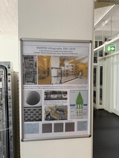
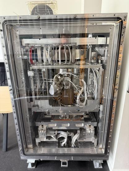
🇳🇱🚲🌷& 🍪 A trip to the Netherlands is never a wasted opportunity to nerd out on semiconductor technology. A thesis defence brought me to TU Delft, but this time I was not gonna miss the opportunity to see the Mapper machine!
🎬 Story time!
🇳🇱🚲🌷& 🍪 A trip to the Netherlands is never a wasted opportunity to nerd out on semiconductor technology. A thesis defence brought me to TU Delft, but this time I was not gonna miss the opportunity to see the Mapper machine!
🎬 Story time!
The company secured some key orders such as Global Foundries that works to tape out critical US DoD chips that end up in things like fighter jets or missiles.
But at the end of 2018, the company was running out of money. Making lithography equipment is very capital intensive and the machines were not selling fast enough. Mapper was looking for a buyer.
Prospective 🇨🇳 buyers were showing up, and that freaked out Washington.
The Pentagon contacted the 🇳🇱 Ministries of the Economy and Defence, the message was clear: "China can't buy Mapper”. This was escalated to Mark Rutte over the Christmas holidays of 2018.
The Dutch government, under US pressure, required ASML to buy Mapper. Since ASML had no interest in multibeam & was all-in on EUV, the Mapper engineers were re-assigned to metrology projects, inspecting the chips instead of producing them.
ASML still operates a small office out of Delft, which happens to be at the ex-Mapper office.
There were only 2 working machines produced, one of which is the one that was rescued by Kampherbeek and TU Delft professor Kruit, and can be seen on campus.
Today, it occupies an important role in Dutch history as the moment the government woke up to the critical role its companies were playing in the geopolitical world of chip production 🍪
The years since have only exacerbated this further
🔚

The fact that the Netherlands, via ASML, utterly dominates high-end lithography for chip production is amazing and pleases me.
It also hammers home the importance of close international trade alliances and the foolhardiness of the "reshoring" efforts for industry generally and chip production in particular. Much longer rant than I have space for here.
Was unaware of Mapper. Next time I am in Delft I may see if I can visit! Thanks for the background and pics.
@fj oh yeah it was.
I‘m not sure I would qualify the mapper solution as „elegant“ - I would say it was its own kind of batshit crazy. And the mapper engineers were some of the smartest people I ever met. 250 people achieving something equivalent of what ASML took 10.000.
@fj NO!
THERE WERE 0 documents emailed inside mapper. I‘m not kidding.
Instead there was „CMT“ - configuration management tool. A simple website with a simple upload button and a search bar. Every file had a unique URL, and you could upload newer revisions of a file and link to either the lasted revision or a specific one.
Literally anything was always in CMT. NOTHING was ever emailed.
@fj You might ask: „How were the files organised? Did you use folders or sth?“
Good question. No folders. None.
Instead, there were design files and a strict naming scheme. And for the machines, the design files told you how things to be done and there were build lists that then gave you info on a specific info. Everything was then documented in Excel files that then linked to the other files (all through CMT unique links).
@fj the most jarring thing in the beginning definitely was „no folders, no start page, no emailing files, no. You start with a build listing which you can see according to which design documents which subsystem was built with which build list“.
It was really cool once you got the hang of it.
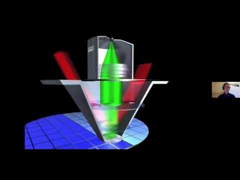
@fj ha, and a MEMS element that was planned to contain 15000 holes, where each individual hole had two sides of a capacitor around, one connected to a light diode, to which a glass was connected. This would then bundle into the „fiber tree“ that went to the FPGA rack.
You had to use light because you can‘t use electricity when you‘re soothing electrons at this MEMS element. Once the beam went through these holes, you could control every single hole individually whether it would deflect or not.
@fj and the beams would continue and then either go through a separate hole sheet and hit the wafer that was moving or be going into the beamstop.
There is a great video about that part on YouTube: https://youtu.be/H8RA5QYT9jQ