TI Debuts MSPM0G5187 and AM13Ex Edge AI Microcontrollers with TinyEngine NPU
TI Debuts MSPM0G5187 and AM13Ex Edge AI Microcontrollers with TinyEngine NPU
Heroic Efforts Give Smallest ARM MCU a Breakout, Open Debugger
In today's episode of Diminutive Device Technology Overview, [Sprite_TM] is at it again - this time conquering the HC32L110. A few weeks ago, we have highlighted the small ARM Cortex M0+ microcontroller, which is outstanding because of its exceptionally small size. We also pointed out a few hurdles, among them - hard-to-approach SDK and documentation, and difficulties making and assembling a PCB for such a small BGA. Today, we witness how [Sprite_TM] bulldozed through all of these hurdles for all of us, and added a few pictures to our collective "outrageous soldering" galleries while at it.
First, he figured out an example layout for this MCU that's achievable for us even on a cheapest 2-layer board from JLCPCB, keeping distances within the generic tolerance standards by snubbing out a few pins. As a result, we only lose access to four GPIOs - those will have to be kept as inputs, so that nothing burns out. However, that's the kind of tradeoff we are okay making if it helps us keep our PCB small and lightweight for projects where these factors matter. After receiving the resulting board, he also recorded a short tutorial on soldering such packages at home with a mere hot air gun and a few bare necessities like flux and tweezers - embedded below.
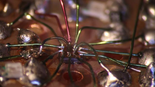
It doesn't end there, however, as he decided to work around the GPIO fanout limitation in a non-intended way. Evidently, [Sprite_TM] decided to have some fun, taking a piece of regular 0.1″ spacing protoboard and deadbugging the chip with magnet wire, much to our amusement. The resulting contraption, pictured above, worked - and this is ever something you'd like to be able to achieve yourself in times of dire need, whether you make something work or simply to be entertained by making use of a cursed mounting technique, there's an one-hour-long livestream recording of how this magnet wire contraption came to be. And, of course, that wasn't the last thing to be shared.
As a finishing touch, he has published bindings and wrappers for Huada SDK so that the chip is usable with GCC, GDB and OpenOCD. He also added datasheets to the same repository - auto-translated but quite readable. All-GPIOs-involved blinkie GIF of a magnet-wire-bound chip triumphantly concludes the write-up.
An addition to [Sprite_TM]'s toolkit is an addition to everyone's toolkit - the techniques, the insights, and the are all here for us to learn from. If you ever doubted your ability to work with small packages in general or this MCU specifically, now you have a whole lot more material to draw upon!
Wondering what kind of miniature device you might want to make? We hackers have mostly been having fun so far, building things like the USB-cable-hidden RubberDucky or a miniature PDP11, but there must be applications in, say, the wearable or medical fields where such a small MCU would prove itself to be a hacker's friend. Maybe you want to build an LED engagement ring with some Cortex-M0+ smarts? In fact, this microcontroller is small enough that it wouldn't be hard to hide inside your PCB itself.
#arm #howto #parts #armcortexm0 #armm0 #bga #chiponboard #chipscalepackage #cortexm0 #hc32l110 #huada #newpartday #sprite_tm #wcsp #wlcsp
New Part Day: Smallest ARM MCU Uproots Competition, Needs Research
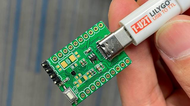
We've been contacted by [Cedric], telling us about the smallest MCU he's ever seen - Huada HC32L110. For those of us into miniature products, this Cortex-M0+ package packs a punch (PDF datasheet), with low-power, high capabilities and rich peripherals packed into an 1.6mm x 1.4mm piece of solderable silicon.
This is matchstick head scale computing, with way more power than we previously could access at such a scale, waiting to be wrangled. Compared to an ATTiny20 also available in WLCSP package, this is a notable increase in specs, with a way more powerful CPU, 16 times as much RAM and 8-16 times the flash! Not to mention that it's $1 a piece in QTY1, which is about what an ATTiny20 goes for. Being a 0.35mm pitch 16-pin BGA, your typical board house might not be quite happy with you, but once you get a board fabbed and delivered from a fab worth their salt, a bit of stenciling and reflow will get you to a devboard in no time.
Drawbacks? No English datasheet or Arduino port, and the 67-page PDF we found doesn't have some things like register mappings. LILYGO promised that they will start selling the devboards soon, but we're sure it wouldn't be hard for us to develop our own. From there, we'd hope for an ESP8266-like effect - missing information pieced together, translated and made accessible, bit by bit.
When it comes to soldering such small packages, we highly recommend reflow. However, if you decide to go the magnet wire route, we wouldn't dare object - just make sure to send us pictures. After all, seems like miniature microcontrollers like ATTiny20 are attractive enough of a proposition that people will pick the craziest route possible just to play with one. They say, the madness of the brave is the wisdom of life.
We thank [Cedric] for sharing this with us!
#arm #microcontrollers #parts #armcortexm0 #armm0 #attiny20 #bga #chiponboard #chipscalepackage #cortexm0 #hc32l110 #huada #newpartday #wlcsp
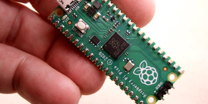
Raspberry Pi RP2040: Hands-On Experiences From An STM32 Perspective

Bare-Metal RP2040: Hands-On Experiences From An STM32 Perspective
The release of the Raspberry Pi Foundation's Raspberry Pi Pico board with RP2040 microcontroller has made big waves these past months in the maker community. Many have demonstrated how especially the two Programmable I/O (PIO) state machine peripherals can be used to create DVI video generators and other digital peripherals.
Alongside this excitement, it raises the question of whether any of this will cause any major upheaval for those of us using STM32, SAM and other Cortex-M based MCUs. Would the RP2040 perhaps be a valid option for some of our projects? With the RP2040 being a dual Cortex-M0+ processor MCU, it seems only fair to put it toe to toe with the offerings from one of the current heavyweights in the 32-bit ARM MCU space: ST Microelectronics.
Did the Raspberry Pi Foundation pipsqueak manage to show ST's engineers how it's done, or should the former revisit some of their assumptions? And just how hard is it going to be to port low-level code from STM32 to RP2040?
How Hard Could it Be?
Raspberry Pi Pico RP2040-based board, hooked up to a Raspberry Pi SBC acting as SWD dongle.
Long story short, after the RP2040 caught my eye, I figured it might be interesting to try and port my C++-based STM32 framework to this new MCU. Not so much for the dual Cortex-M0+ cores, though, as I have STM32H7 dual-core (M4 & M7) MCUs lying around which will handily beat the stuffing out of an RP2040 with gobs more I/O to spare. What mostly intrigued me was this state machine peripheral (PIO) in the RP2040 that seemed worthy of a closer look.
Based on my experience with STM32, I figured I could quickly port over some files, create a new 'RP' architecture branch in the project and be off to the races. Cortex-M is Cortex-M, right? The usual procedure with a new ARM-based MCU is to get the datasheets, reference manual and the CMSIS device files. After this one can easily adapt the low-level code to use the new peripheral naming & register layout, while core-level devices (SysTick, NVIC, etc.) stay the same.
Perhaps naively, I had put in an order for a Raspberry Pi Pico board before even checking for CMSIS support, or glancing at the reference manual. To my surprise, I found that CMSIS support or even interoperability with the rest of the Cortex-M ecosystem was not yet on the radar. Still, the SVD file for RP2040 MCU is provided in the 'Pico SDK', which can be used to generate the device header from. Courtesy of Chris Hockuba's efforts on bootstrapping CMSIS with the RP2040 I eventually had a working solution together.
This Could be Easier
RP2040 boot sequence (RP2040 datasheet, Fig. 15).
With an STM32 project, there are a few items required to make a bare-metal project work on a target MCU. These include the start-up code which performs some basic setting up of the environment as well as the vector table for interrupt handlers. There's also the linker script to ensure that all bits end up at the right memory offset. This is all fairly minimal, with the MCU upon boot loading the firmware image from Flash ROM at the default address.
The first hurdle with the RP2040 is to understand its chained bootloader process. Much like with bootable floppy disks of yore, or a HDD/SSD in a PC, the external QSPI Flash ROM is treated essentially as a potential boot device by the MCU. The first stage bootloader is integrated into the MCU in boot ROM, address 0x0000 0000, which upon boot checks the QSPI interface to try and load 256 bytes from it. This will be checked for a valid CRC32 hash match and assumed to be the second stage bootloader if it matches.
There are a lot of things which this second stage bootloader could do and some which are required. Suffice it to say for now that compared to some famous STM32 clones - such as the GigaDevices I-can 't-believe-it's-not-a-genuine-STM32 clones - which also use SPI ROMs, this whole process with the RP2040 is not as intuitive, well-documented or transparent as it could be, with plenty of stumbling blocks.
Good Artists Copy
It took me a fair bit of digging around in the RP2040 datasheet and asking around to figure out how the peripheral clock manager in STM32 maps to the RP2040 system architecture. As it turns out, the RP2040's version is called RESETS and works basically in reverse: you have to unset the reset condition on a block to enable the clock for it. To enable the GPIO clock, you have to toggle bit 8 in RESETS_RESET (PADS_BANK0).
Block diagram of an RP2040 GPIO pad.
That figured out, I looked at the GPIO peripheral section in the documentation (section 2.19). One thing is immediately apparent: this is completely different from the STM32, AVR, SAM and most other GPIO peripherals I have ever seen.
While most chips have one or two registers per function, and you shift bits into them to activate that function for a particular pin, the RP2040 has a register per pin and you shift bits into a place that dictates the function. It's a unique choice, and I had to write some custom code to look up the memory address of the control registers for each pin.
After going through all of this effort, surely it will just work, right?
Boot Shenanigans
As mentioned before, the second stage bootloader has to be located at the beginning of the firmware image. Since I figured this had to be some generic code, I simply took the ready-to-use ASM code that got spat out by the official PicoSDK while building the Blinky example. With this added to the RP2040 Nodate port, the Blinky example built without issues.
Flashing the resulting ELF binary to the RP2040 was the next challenge, as there is no onboard ST-Link-style SWD adapter on the Raspberry Pi Pico board, and as a dual-core Cortex-M MCU, it requires a multi-drop SWD adapter. So far the only multi-drop SWD adapters which I have are integrated on STM32H7 Nucleo boards. Thus I decided to use the custom OpenOCD fork which was created by the Raspberry Pi Foundation, running it on a Raspberry Pi SBC.
With all that in place, I successfully flashed the firmware to the RP2040 and… got absolutely nothing. From a cursory inspection it appeared that the code never got past the initial boot loader and into the actual firmware in the SPI ROM. Whether this is due to an issue related to the second stage bootloader ASM, something in the experimental RP2040 CMSIS files which I had to borrow from someone else's efforts, or due to something else entirely is hard to say at this point.
To Be Continued?
After spending quite a few hours on making bare-metal RP2040 work using cobbled together CMSIS and second stage bootloader files, it felt like the right time to take a few steps back and reevaluate. Since my initial evaluation of the RP2040, the CMSIS feature request in the Pico SDK tracker has joyfully been updated with the suggestion that official CMSIS support may be added with the 1.2.0 release of the Pico SDK.
I think it makes sense for anyone who wants to get intimate with the RP2040 using industry standard tools to wait for this release. Once it drops, I'll likely end up revisiting first the Nodate Blinky example, and then finally check out the PIO peripheral. Having read up on its two state machine architecture, it seems interesting enough. Not as powerful as a CPLD or FPGA, but still extremely useful.
The single RP2040 'datasheet' (more a reference manual & datasheet mashed together) seems to at times forget that it's supposed to be covering the MCU, and will veer off into being a Pico SDK tutorial. While useful for those who wish to use the SDK, it's decidedly less useful to those who are writing their own implementation.
From the convoluted GPIO peripheral, the complicated multi-core boot process, and the added hurdle of having to integrate a second stage bootloader along with a non-transparent external ROM, much of it rather grates. You're going to want to use the official SDK.
It's possible that once one gets used to these design choices, it won't feel as jarring. Or maybe it's just a question of working the RP2040 into the standard toolchain. Every new MCU is a bit of a learning experience, after all.
#arm #hardware #microcontrollers #armcortexm0 #cmsis #raspberrypi #rp2040 #stm32