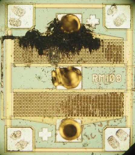
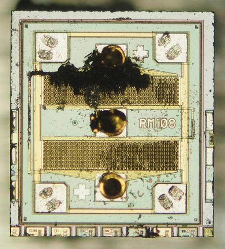
Here's a die shot of an RF MOSFET I fried. It's supposedly a Motorola RD01MUS1 (but could be a clone/fake).

I don't have (or want!) the chemicals to de-cap it properly so I tried the method of overheating the package & cracking it apart with pliers to pop out the die. Aside from a bit of epoxy still stuck to it, it worked out pretty well!

In the wide shot of it, it looks like there were some other designs on the wafer that were sliced through to cut this one out. (or maybe just test patterns?)
@miek The stuff along the south edge is pretty clearly vernier patterns for inter-layer alignment, very common especially on older nodes using contact litho
@azonenberg ahh, thanks!
@miek @azonenberg right edge looks like a transistor test structure
@miek @azonenberg with pads large enough to hit with a flying probe or a wire bonder