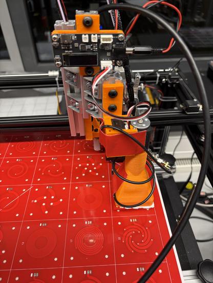
I've got a new #KiCad plugin out in the KiCad plugin manager:

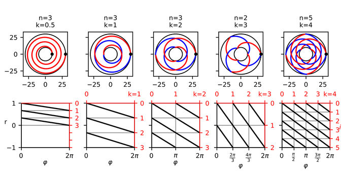
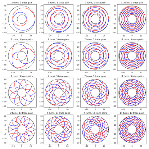
KiCoil generates "twisted" planar inductors. You can make it do one- or two-layer spiral inductors, toroid inductors, and many intermediate, hybrid variants in between spiral and toroid inductors.

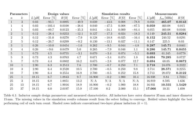
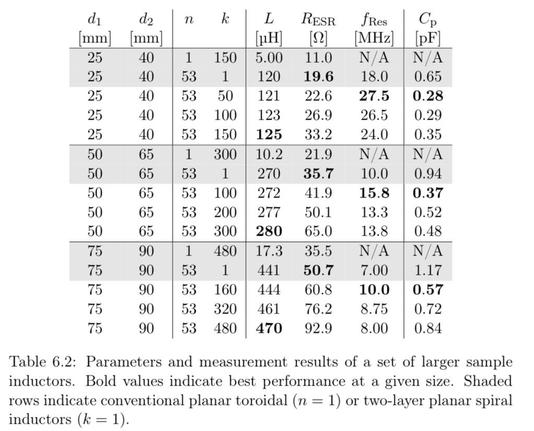
These hybrid types have wider traces than a single-layer spiral, and have better high-frequency behavior (parasitic capacitance and self-resonant frequency) compared to two-layer spiral inductors. And they look really pretty!

#electronics

@jaseg out of curiosity, what's a typical inductance that you can sensibly achieve with these?
@gsuberland Depends on board area, I'd say about 50 µH in 25 mm diameter and maybe 400 µH in 50 mm diameter. The main limiting factor for large inductances is DC resistance due to the narrow trace width you need to stack many windings.
@jaseg @gsuberland huh, but thats already feasible sizes for SMPSes, neat

@funkylab @gsuberland I think the main limitation using these for something like an SMPS would be that they are coreless and large, and as such they would be a total EMI nightmare if you fed them straight from a FET switching with nice, crisp edges. You could maybe mitigate that and increase inductance with one fo these ferrite shielding sheets you can get for cheap for wireless charger coils.

Besides that, when pushing power, in PCB planar inductors the DC resistance quickly gets annoying.

@funkylab @gsuberland btw, the GUI calculates a rough approximation of inductance. The approximation holds for near-spiral layouts, the closer you get to a toroid the higher the real inductance gets compared to the calculated one.
@jaseg @funkylab @gsuberland Have you done any characterization against real PCBs? If so, can you share some results and pretty pictures?
If I have empty PCB space on a future project, I would put some of these on there just for the looks.
@tom_verbeure @funkylab @gsuberland I have, a detailed analysis is going to be in my PhD thesis which will be public in a few months, but I can find the results table and post a screenshot here.
@tom_verbeure @funkylab @gsuberland
here’s the results for various configurations of planar spirals with 35 mm size (pic 2) and various larger toroidal-ish configurations (pic 3). The measurements were done on a keysight handheld LCR meter (ESR, L) and a nanoVNA (SRF). first pic is the measurement setup I used to determine their coupling symmetry in a wireless power transfer configuration.

@jaseg Thank you very much for sharing these ideas and measurements.

I am also intrigued by the machine shown in the first photo, with the articulated arms and the orange 3D-printed parts. I would be curious to better understand how it operates and what its objectives are. Does the articulated arm move across the different planar toroid prototypes to characterise their behaviour, or to measure the effects under various positions? Is that the idea?@tom_verbeure @funkylab @gsuberland

@allainyann pretty much, it's a modified 3D printer. I bolted a thing to the toolhead that holds a coil that it can rotate with a servo. The big board on the bottom contains a bunch of different coils. By moving over one of them in XYZ and rotating the coil on the toolhead, the setup can then measure coupling of two of these coils depending on misalignment and distance.
@allainyann The goal of this setup was that I needed two small turn count inductors for a wireless power transfer setup in which one of the coils rotates. In this setup, a conventional spiral coil produces a slight ripple on its output that changes with rotation because the spiral isn't perfectly rotation-symmetric. By "twisting" the coil, you can reduce that ripple.