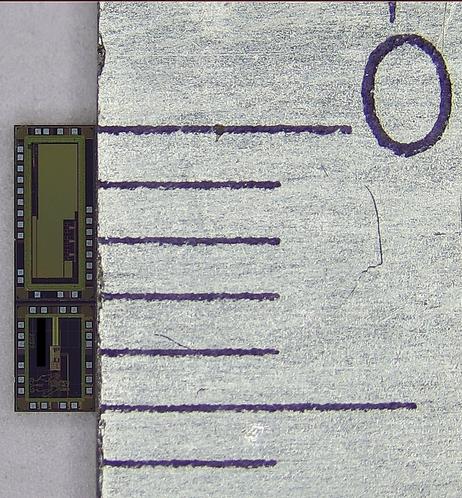
So here are the photos of the actual chip, taken with a microscope. The black rectangle censors my name. I placed a steel ruler next to the chip in one of the photos to give you an idea of how small it really is. Each black line corresponds to 1 mm

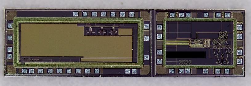
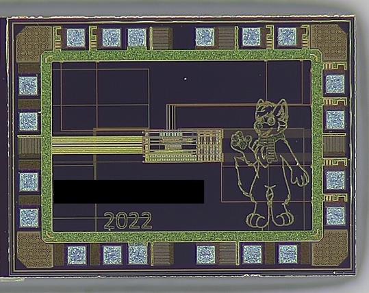
The artwork on the chip is from OggyTheFox (@oggythefox.bsky.social on Bluesky)

In the second picture, you can see that there's always a second chip next to my chip. I don't know what kind of chip it is or why it wasn't separated from mine, but it at least makes the whole thing a little easier to handle because it makes it physically larger x3

I have five chips without a package and five have been bonded into a package, so I'm currently designing a PCB so I can test if the chip works :3

#electronics #asic #asicdesign

@Polarie_Fox Wait wtf you designed the silicon?! :O PCBs are already complex and difficult enough for me xD

@ntoskrnl

Basically, yes :D

But it's similar to designing a PCB, except that instead of using ICs and other passive components, you have a library of building blocks such as different types of flip-flops or other logic gates. You can customize each individual transistor, but this is usually not necessary, especially in digital circuits. The chip I designed for my master's thesis required more customization. I needed a differential amplifier for the circuit and had to build it myself, calculating the length and width of each transistor gate to achieve the desired behaviour

@Polarie_Fox okay THAT is crazy fucking cool. nicely done :D