presenting without elaboration
that 1k through-hole resistor is there becaussse it was either have a resistor do double-duty as a jumper wire, or switch to a four-layer board just for one trace.
not a good solution but maybe the least-bad.
update:
realized wait, LTspice can totally calculate power dissipation; I ought to see if my components are gonna cook.
fine: MOSFET drawing somewhere like 12-15W which is A Lot but I planned for a heatsink.
probably not-fine: >10W on an 1808 capacitor, 400mW on a 0603 resistor
🌶️ ♨️ 😅
me: i need to think very carefully about this board layout and I want things to be clean as possible.
other folks, with apparent success:
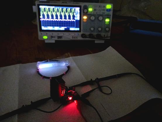
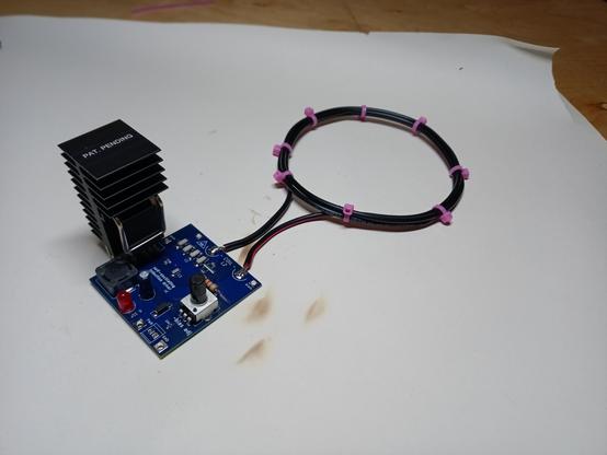
The field-wiggler is operational, at least partially.
Pictured: wirelessly lighting an ampoule of neon.
Problems:
- getting some higher frequency noise on the mosfet gate, probably some sort of parasitic resonance. May or may not be significant.
- drive coil gets *really* hot, fast. 18ga wire apparently isn't adequate for this much RF power?
- I've blown up three out of my five mosfets (and that's not an inexpensive component). Worse, I'm not sure exactly *why* they've failed.
I could buy litz wire.
(Thanks @Hearth for offhand mentioning litz wire years ago!)
Ultimately though I do want this to be a PCB coil which should be fine? 1oz copper traces are 35μm thick so standard current-capacity calculator tools should be applicable.
Decided to play with this device a bit more.
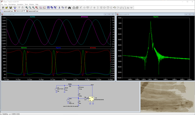
Characterized my inductors, made another inductor with only two turns instead of three. I don't have an LCR meter so uhh used the 1kHz calibration output on my scope to ring a little parallel-LC resonator circuit and measured the frequency.
To my great surprise, I also found that the device performs much better at ~12v than the ~20 that other folks have run previously.
Still not sure what exactly is causing the ~100mhz ringing.
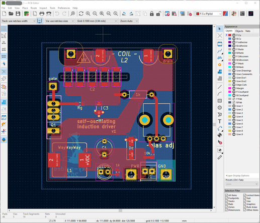
@s0 the funny thing is I'm pretty sure that resistor is totally superfluous, but folks before me have put it in their designs so I thought why not.
I do need a jumper there though because the next-best routing option would have been to split my ground plane directly under an RF power trace.

update on the ~100mhz ringing:
thought about it some more, and did some more poking at LTspice. While the previously highlighted axial resistor might well be inductive, it's hardly conducting any current. Not nearly enough to produce that kind of oscillation.
My new suspect: the parasitics on the mosfet itself (plus a bit of pcb trace) are acting as resonant LC circuit. Turns out this is totally a known phenomenon if external gate resistance is too low. I had been thinking of my 2Ω2 gate resistor as part of a phase-shift RC circuit (that's how it was presented in previous work I'm referencing), but it also is dampening the parasitic LC resonance.
Here's a video of a lovely gentleman going in-depth on mosfet gate ringing and necessary resistor values

should be able to test this tomorrow.
and I'm... having this feeling like I've rapidly departed from "dabbling at some electronics" and entering territory of "this legitimately qualifies as electrical engineering".
it's a funny feeling.
goddammit blew up my last FET.
What I'm tempted to do is order more of them and keep fucking around.
What I should actually do is redesign this board based on lessons learned and include some more self-protection features.
problem: no overvoltage protection on the mosfet gate
plan: add zener/TVS clamping diode
problem: mosfet failure to oscillate creates possible overcurrent condition
plan: current-measuring shunt + op-amp + etc to force mosfet gate low if device overcurrent
problem: layout is kinda bad for parasitics.
plan: make the layout less bad.
swear someday I'm gonna do my best to explain wtf is going on for all the non-electronics critters who so kindly follow me
in the meantime this is raw projectblogging
me: what's the deal with HV creepage (arcing/breakdown) distances under surface-mount capacitors? Seems to violate IEC design guidelines for minimum space
high-spec capacitor mfg: Hey here's some information about this exact question.
https://www.johansondielectrics.com/impact-of-pad-design-and-spacing-on-ac-breakdown-performance
like this is something that seems particular for electronics part manufacturers, even moreso than most industrial products:
they go out of their way to show you *exactly* how best to use their shit.
It makes learning about how to actually make stuff so, so much easier. You might need to wade through a forest of datasheets and application notes, but information is the opposite of obscured.
what people think electronics design is: routing pcb traces, brandishing a soldering iron
what it actually is (much of the time): squinting at poorly-photocopied performance curves in AZ23C51OMGWTF.pdf with calc.exe open on the 2nd monitor.
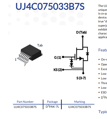
All right, so, I have this mosfet which I expect to be dissipating a fair bit of power (several watts, potentially >10W). In the previous prototype I used a THT part (SO-247) with a bolt-on heatsink, which worked pretty well.
Ultimately I'd prefer to use a surface mount part, and the device is also available in D2pak-7.
My plan was attach the tab to an oversized pad, drop an array of thermal vias to the ground plane on the opposite side, and mount the entire (single-sided) board's ground plane on a shared heatsink.
The problem is the thermal tab on this device isn't connected to ground, but instead is the pin for Drain. So I can't drop thermal vias to the ground plane.
Is the expectation that I use a top-mount heatsink, dissipate heat through a big power plane for Drain on the board's front, or what?
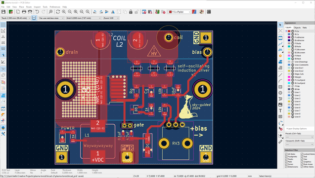
Here we go, a Revision 2 of the board! I think it's ready to send to the fab, but inevitably I'm gonna find some small things to tweak after posting.
Light blue rectangle is the outline of a big heatsink on the back side of the board.
Thanks to @gsuberland and @electronic_eel for their input on thermals :)
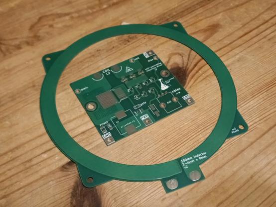
new boards already arrived!
ngl I'm a bit spooked by how fast and I
inexpensive it was, even though there's pretty explicitly some kind of promotional/loss-leader pricing going on.
Also these are 0.8mm boards (half of "standard" thickness) which should help with both front-back thermal conductivity and make the two-layer inductor a little more inductor -y.
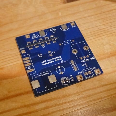
oh yeah, seen in action here is a hot tip I'm only recently internalizing:
if you're making a thing and it has screw and/or mounting holes, mark the screw size/spacing directly on the object if at all possible.
@skyguided That's a lot of via stitching! Probably pretty necessary though.
If you can afford to make the source pad larger too, a little bit of heat can be dissipated that way--it doesn't *all* go out the thermal pad
-F
@skyguided didn't you want to put a TVS diode near the gate to protect it from overvoltage? I would put it directly next to the gate, to prevent any trace inductance from delaying it's action.
also i would add a row or two more of vias to the source, the 6 pins aren't that bad at conducting additional heat.
@electronic_eel I did add an additional row of thermal vias after posting this.
Though now I'm also realizing I don't know why I put the TVS (D3, the little SOT23) on the distal side of the gate resistor :/
@skyguided yeahhh it's kinda Hard
one of our coworkers swears by these things called "thermal jumpers" which are little SMD parts that are thermally but not electrically cnductive, so you can use them to connect that drain to an adjacent ground fill and then go from there to the backside
-F
@skyguided there's also this style of heatsink: https://www.digikey.com/en/products/detail/boyd-laconia-llc/573300D00010G/1216345
which is designed to be used like the image below, taken from the boyd catalog
they're not capable of handling a lot of power, but if you need just a little bit more heatsinking than your board allows, you can use one of these
-F
@skyguided and then the other other option is to use one of these MOSFETs, where the thermal pad (still connected to the drain, i'm afraid) is on top, so you can just attach a normal heatsink to it
@skyguided tab on drain is common for these kind of FETs.
Do you really need the ground plane right below the FET? You could make a cutout there and have a drain area that is connected with the thermal vias. Then use a thin silicone pad or similar between the bottom pcb side and the heat sink for electrical isolation. Maybe go to 4 layers if you don't want to make a cutout in the ground plane.
@s0 :nod: I could bolt a heatsink on the top side for sure, but I think it'd be a big heatsink on a relatively small chip which feels a bit funky mechanically.
That foam is intriguing
@skyguided Even better when you get a sufficiently old piece of equipment and the manual is a 500-page book with complete schematics, theory of operation, and "here's exactly how to fix this if it breaks in these common ways"
as long as you can find a copy of the manual, anyway
i wish they still did this
-F
@skyguided (Tesec is also the kind of company that still makes brand new, 100% compatible units of their 8088-based all-analog-except-the-computer-interface tester that they first made in the 80s. the only reason they're not the exact same thing is that mercury-wetted relays are no longer legal.
no one else does that! more people should do that!)
-F
 that’s great
@electronic_eel @s0 oh heck, new year
Yeah that's a good point
@skyguided You've gone past "legitimately qualifies as electrical engineering" and right into "most EEs think of this as black magic", honestly
the majority of electrical engineers don't do much of anything RF--these days, it's mostly all digital stuff.
-F
 resistor?
 secret inductor.
