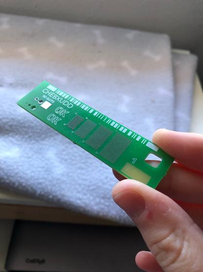
someone should make a jlcpcb bingo card. so far iโ€™ve got

โ€œasked to confirm thereโ€™s no copper in my gerbersโ€

and

โ€œincurred the fee for too many slotsโ€

@jacqueline I've wanted to make a PCB fab stress test board
@xssfox @jacqueline now I want to too.
@martin_piper @xssfox if you ask aisler nicely then they will send you some if theirs. they make super neat little conversation pieces re: the challenges of pcb production
@martin_piper @xssfox (my fav thing about this -- something i didn't previously know -- is that the closest trace width on this board is designed to fail. if those traces don't bleed into one another, then they haven't put enough copper on the panel or w/e
@jacqueline Do they test those coppered areas against a standard capacitance? It seems like it'd be a great way to confirm the spacing between the traces.

@brendan idk but we can ask @aislerhq

the does sound pretty clever tho

@jacqueline @brendan We just electrically/optically inspect the coupons.
@brendan @jacqueline It's not just about the spacing, but also about how those traces' edges look: How rough they are, and what their profile looks like, if they have an angle. Capacitance is only going to image a fraction of that.
@jaseg @jacqueline a frequency vs reactance plot would probably be pretty sensitive, but not straightforward to interpret. I can see why they do optical inspection.