This was a close shave. Almost couldn't fit both JTAG cables next to each other.
I verified non-interference of the board side male connector but forgot the female IDC connectkr overhung on the sides.
Bringup is going pretty well I think.
Maybe could use a bit more kapton tape?
Gradually bringing up firmware on the main MCU. UART, uptime timer, and config variable database are running, about to work on the link to the FPGA.
But first I need to do a bit of independent testing on the FPGA.
Just loaded a test bitstream on the FPGA and verified the LEDs all work. And the supervisor is able to see when the FPGA is up.
Next step, I think, will be getting the MCU and FPGA to talk to each other.
Got a stripped down version of the base FPGA bitstream running.
It's super nice having all of the data from different instrumentation all coming to one place in ngscopeclient so I can have a single dashboard to look at everything.
After fixing a few PEBKAC issues, MCU and FPGA are talking over quad SPI.
But the data coming back is shifted by a nibble or two from what I expect. Not yet sure if timing or logic issue.
Should have put test points on the QSPI bus but silly me thought that since it worked last time, I'd be fine with PHY layer stuff and could just use an ILA on the FPGA...
And they're talking properly! That's it for tonight, I have to be awake in five hours...
I'll probably work on thermal stuff after work, since that affects the health of the rest of the board. The tachometer output of the fan goes to the FPGA (for... reasons) so I need to implement a speed monitoring block and make it output RPM values over QSPI to the MCU.
Then I need to add a PWM generator on the MCU, and bring up an I2C bus to poll the four temperature sensors around the PCB.
Also I found a new design oversight.
I have monitors for the supervisor on every regulator PGOOD pin so I can detect and shut down if a rail starts sagging due to overcurrent etc.
But I don't have an ADC pin on the 12V input so I can't detect a failure of input power and sequence rails off properly. All I can do is wait until one rail trips out of regulation then panic shutdown the rest (without proper sequencing delays since this is indistinguishable from a short).
I2C4 isn't happy. Trying to read the MAC address EEPROM and getting hung up sending an I2C start bit. The register is supposed to be self cleared in hardware and I'm not seeing it ever clear.
So either there's a peripheral setup issue (nothing jumps out at me in a quick register dump) or something is wrong in hardware (SDA or SCL stuck/open).
Unfortunately this bus is on internal and back side routing exclusively (again, should have put a top side test point on... Derp). So I'm gonna have to rip off some tape and invert the board when I get home from work and see what's really going on.
Started a google doc with a live "things to do better next time" list. So far all are minor annoyances or things I can work around without having to bodge the board. (Anyone have a self hosted, lightweight suggestion for this kind of thing? Etherpad or something?)
https://docs.google.com/document/d/10j4HWuMBLfLvX5Notvezs26lcIxuNnWbeJlv_JciUEA/edit?usp=drivesdk
The I2C4 issue smells like a soldering issue so far, but I'll know more when I get home and land probes on the bus.
My main bench scope is out for service still so I'll need to use the 16 GHz monster to troubleshoot my I2C. Miiiiiight be slight overkill...
(I could also use the PicoScope but it's on the other side of the bench, not sure if probes will reach all the way over here)

LATENTPINK bringup notes
LP2996 needs to be powered by 3v3_SB so AVIN is up before PVIN Provide 2 way comms bus (i2c?) From super to main mcu for querying rail status and requesting warm reboots/shutdowns Move supervisor to stm32l031 qfn48 package (need to buy some) to get more IO capacity Hook FPGA done pin to main MCU...
Back from work and debugging the I2C issues.
I2C1 (temp sensors) is giving NAKs to any bus access while I2C4 (mac addr eeprom) hangs trying to send a start bit.
Probing I2C1 at the pins of the temp sensors shows SDA stuck at 0 while SCL is floating high as expected. Wonder if I have a bad solder connection on the pullups?
Time to pull some tape and cables off the board and get it back under the microscope.
OK, that explains everything.
Misread the alt function table and had PB6-PB9 set to AF4.
Turns out that while AF4 is I2C4 on some other pins, on PB8/PB9 it's... I2C1.
So I had two sets of pins muxed to the same peripheral and Bad Things(tm) happened, including traffic going out the wrong pins (gee, I wonder why it never got acked...)
Yep, this looks more sane.
The FPGA -> MCU QSPI link probably needs some timing tweaks still; it works at 25.6 MHz but when I try to bump it up to 32 or 42.6 MHz I start seeing results shifted by a nibble.
Will troubleshoot that later, I don't need more than 100 Mbps of MCU-FPGA throughput now (if ever).
Next step will be building the fan tachometer in the FPGA, I think.
Tachometer core on the FPGA builds OK but is giving values that are way off the ~5k RPM I measured for the fan with a scope.
Not yet sure why. The tach block integrates N (currently 16) cycles of the waveform, measuring period against a stable reference clock, then converts frequency from Hz to RPM.
I have a dead time (currently 1000 clocks at 187.5 MHz, so 5.3 us) after each toggle for debouncing which might be too short. Or maybe it's a math error converting from Hz to RPM. I'll find out tomorrow.
Turns out that while I did have a small math error (two *pulses* per revolution on the green wire, not two *toggles* per revolution), the main error was actually in my bit-serial divider IP.
Which I had written back in grad school for my thesis, and it worked great on that CPU because I happened to have the inputs stable from when a divide was issued until it retired. The interface spec called for the divider to register the inputs on the first cycle, but one line of code used the unregistered value instead. Oops!
Anyway, I now have working fan tachometers (no PWM outputs yet, so they're always at max RPM), plus I can read the FPGA sensors using the XADC, and the I2C sensors scattered around the board.
The STM32 also has an on-die temp sensor which I'm not using yet, but I think that's the only missing bit.
None of the Ethernet PHYs or power supply components have die temperature sensors on them to my knowledge. The SFP+ may have a sensor on its I2C bus, but I haven't brought that up yet (that will come much later).
Also tweaked a few timing settings on the quad SPI and I'm now getting reliable performance at 42.66 MHz (170.64 Mbps). That's as fast as I can go without either changing my FPGA-side QSPI IP to not require 4x oversampling, or moving it out of the RAM controller clock domain into something faster (which would then necessitate a lot more CDC blocks on the core fabric SFRs).
While the sensors are brought up in that they work and I have functions that read them, there's no commands in the CLI to read them later on (yet). So for now all you can get is single-point measurements during boot.
So now there's a few directions I can go for what to bring up next:
* PWM outputs for the fans
* Warm reboot request between main MCU and supervisor
* RGMII management interface
* SFP+ uplink
* SGMII edge ports
* QSGMII edge ports
* QDR-II+ SRAM
I'm thinking the RAM might be good to do next since it's fairly self contained and easy to test in isolation.
While waiting for a RAM test bitstream, wired up a test fixture for sniffing and verifying traffic on the SFP+.
It's just two back to back optics connected through 6 dB RF splitters with the other leg of each going to the scope.
And it's a good thing I checked.
Apparently this wall port is spitting out 1000base-X traffic, not 10Gbase-R.
Time to go fix that before I think about bringing up the 10GbE on this board!
Aha, that would do it. PP4/34 is connected via an obviously temporary patch cable to a 1000base-SX optic on one of my 1G switches. And there's a cable coming off my 10G core switch dangling right next to it.
I must have needed a 1000baseX test signal a while back and forgot to reconnect the cable.
And getting nice looking 10Gbase-R idles coming off the switch now.
The line coming off the LATENTPINK board is flatlined, which is unsurprising as the FPGA design loaded on it doesn't yet bring up any of the transceivers.
It seems all of my simulation testing paid off, possibly? My homebrewed QDR-II+ controller seems to have worked on the first attempt in real hardware!
It uses a fair bit of juice (unsurprisingly, given all of the SSTL signals). Power consumption jumped from 5.5W to 8.2W (2.7W delta) when I loaded the new bitstream, but everything is still happy (FPGA Tj is at 39.5C and seems to be stable).
This is running the RAM at 375 MHz (750 MT/s), comfortably less than the 450 MHz (900 MT/s) speed grade limit. But that's all I need to get 24 Gbps of throughput, which is the requirement for this board to saturate 14x 1 Gbps + 1x 10 Gbps links.
No MIG, no PHASERs, no weird MEMORY_QDR mode on the ISERDES to sample on CQ and CQ# rising edges.
Just using IDDR's clocked by a 90 degree PLL shifted version of CQ/CQ# fed to a single IBUFDS.
Next step will be to write a full BIST core so I can get more confidence than "I poked two addresses in the VIO and it seemed OK".
Started bringing up the SFP+ interface.
The MCU now correctly detects optic insertion/removal and toggles TX_DISABLE a short time after the optic is inserted.
So far RX_LOS is ignored and I don't do anything with the RS pins. The DOM logging is just a test, I won't actually dump all the sensors every time an optic is inserted long term. That will be under "show interface transceiver" or similar (along with lots more details).
But something is wrong, the transmit data seems very unstable and I'm not seeing anything that makes sense.
I think this might just be the optic sending noise with the FPGA either not transmitting at all, or transmitting gibberish. My logic analyzer in the FPGA fabric is failing to arm because Vivado isn't seeing a clock.
Well that explains the implementation warning I was getting about an "invalid clock configuration" that I had been chasing for a while but never found the root cause of.
The transceiver quad PLL had a typo in one setting so it wasn't locking. That explains a lot.
Now linking up and seeing broadcasts on the sandbox network.
SFP+ link/activity LEDs on the board don't currently do anything, so that will probably be the next TODO item.
Note that the eye patterns in the screenshot are taken off the SFP+ mid-span tap, so while they' can be used as a reasonable proxy for jitter in the actual waveform, they won't show small reflections or vertical eye closure present on the actual DUT. At some point I'll probably land probes on the actual differential pairs on the PCB, but for the moment it looks to be clean enough I doubt there's any problem there.
Ok so, the obvious next step is to tie up a few loose ends around the SFP+ uplink (make sure all the low speed control signals are tied off, maybe add some logic to check TX_FAULT, make the link up signal on the FPGA drive the link LED, and add a pulse stretcher for the activity LED).
After that, I think I'll work on bringing up the RGMII PHY on the management port and finish the remaining bits of glue for shoving Ethernet frames over the quad SPI bus so that the STM32 can actually be reached over the network via ping / SSH.
RGMII management port came up on the first try with no fuss. Yet another painless bringup step.
I haven't had to bodge the board at all (although I did solder probes to the I2C pullups thanks to the lack of a designed-in test point on them) which is a slight surprise.
I either did a really good job designing and verifying this board, or there's a catastrophic error lurking right around the corner in one of the subsystems I haven't looked at yet. We'll find out soon!
It's now pulling 8.8W and while temperatures are gradually increasing as I load down the board, they're all well within safe limits:
* SGMII PHY area (both PHYs idle): 25C
* RGMII PHY / 1.2V regulator area (linked up at 1 Gbps, no traffic): 28C
* MCU / 3.3V regulator area: 30C
* SFP+ optic (linked up at 10 Gbps, no traffic): 34C
* QDR-II+ SRAM area: 34C
* FPGA die: 42C
I kinda expected the RGMII PHY to run hotter but right now the fan cooling the FPGA is blowing over it first, so I guess that's helping.
The heatsink on the FPGA seems to be doing its job so far. This is my first board that I designed a thermal solution into (vs running cool, or having one bodged on ex post facto), so good to see it's at least somewhat functional.
That's it for tonight since I have to be up for work in the morning.
Next step is going to be building out more firmware and gateware around the management interface:
* Make the MDIO bus accessible over QSPI from the MCU, rather than just a JTAG debug core
* Finish the FIFO logic and interface code on both MCU and FPGA side, so I can send and receive Ethernet frames from the MCU
* Verify SSH over real Ethernet
Decided to try bringing up the SGMII ports first.
Hmm, i wonder why port g12 wasn't responding? Easy fix with 30 seconds of hot air. Another failed solder joint from that same reel of 2013 era 33Ω resistors. Might be time to retire the reel?
Now it links up fine at gigabit speed, and the SGMII link is up.
But it's not responding over MDIO which is a bit of a head scratcher. I tried bruteforcing the entire 5 bit PHY address space (in case there was a problem with address straps) and got no response at any address.
I'm not sure what's going on here. The PHY is obviously right way round on the PCB, getting power and a clock, and not in reset or power down if all the other functions work.
There's no issue with the FPGA soldering, PCB traces, or RTL; I threw probes at the PHY pins and saw well formed MDIO traffic.
Failed soldering on *only* mdio and mdc, of both PHYs, seems unlikely.
MDC has a good clock so it's fine; MDIO is clearly not shorted/open since it's got well formed headers. It's got a pullup and is sitting at VCCIO during the idle period (when a PHY should respond).
MDC frequency is 2.5 MHz (same as I use for the KSZ9031, but a different bus) which is well below the 25 MHz Fmax for the DP83867.
Touched up every pin on the PHY, one by one with microscope inspection, in case I had a bad solder joint.
No change in behavior.
Still confuzzled. Tried a few more things (hooking up the INT/PWRDN pin to the FPGA with an on die pullup in case having the pin unused in the bitstream did something weird), verified relative timing of MDC and MDIO were sane.
I can't understand how the PHY can be happy enough that it links up 1000baseT to my laptop, has an estimated e-12 BER for the SGMII link to the FPGA (based on 8b10b error and total symbols performance counters), and yet is unresponsive over MDIO.
The only explanation I could think of was a soldering problem that happened to affect those two pins but I specifically resoldered them.
And that wouldn't explain why the second PHY is equally unresponsive.
Found and fixed a power rail sequencing issue (the DP83867 wants its 2.5V analog rail stable prior to the 1.8V analog rail, and I was ramping in reverse order). There is (explicitly stated, not assumed) no sequencing requirement for these rails vs the 1.0V digital core and the VCCIO rail.
No change in behavior with that fixed.
Innnnteresting. Apparently GPIO_0 is a strap?? Let me try pulling that low and see what happens.
Tried a new bitstream with explicit pulldowns on GPIO_0 and GPIO_1.
Reading a bit more, it seems that if GPIO_0 is strapped wrong it will pull MDIO to VCC/2. Which is not what I'm seeing here.
Instead, I'm seeing MDIO tristated and floating high (as if the PHY isn't even attempting to talk to me).
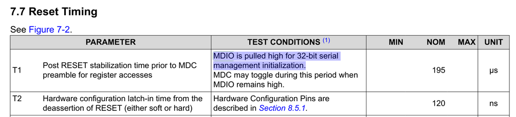
Bootup delay from RST# (blue) going high to MDC (yellow) beginning to toggle. 867 us, datasheet only requires 195 us.
And plenty of toggles on MDC before activity on MDIO (green).
Note that the actual PHY I/O signals are LVCMOS18; I'm probing MDIO at the PHY pins but the FPGA mirrors MDC and RST# to a 3.3V GPIO connector since it's tricky to get too many probes on a little QFN.
I did probe separately to confirm that MDC is reaching the actual PHY pins, and since it's linking up RST# is obviously clearing OK.
Hmmmm, interesting, The VSC8512 isn't responding over MDIO either.
I wonder if it's something about my FGPA-side MDIO controller (weird timing or something) and the KSZ9031 is more forgiving? It's the only PHY I recall having used with it in the past.
Anybody have ideas?
OK, scratch that theory. I just found an old ngscopeclient dataset from my previous experiments with the DP83867.
I had MDIO working successfully using this same controller on it. In that particular case I was running at LVCMOS25 levels rather than the LVCMOS18 I'm using here, but it was the same FPGA IP.
So clearly the DP83867 *is* able to work with my controller. Which makes me lean back towards a hardware issue again.
But I'm still at a loss as to what could make MDIO fail but literally everything else work.
Actually no, the PHY *was* running at LVCMOS18 levels. The FPGA was using LVCMOS25 and I had a level shifter.
So almost every single thing was the same on that board vs here. What changed??
Awake for the day and troubleshooting more.
The remainder of the PHY is working fine, for sure. The fabric CDR block is locked and I'm getting valid 8b10b symbols.
After letting it run overnight, I have 5.1e12 symbols received without error on g13 (baseT link down) and 5.12e12 symbols with 71 errors on g12 (baseT link up). This is unsurprising as with the link up there's more power consumption, noise, variability to the data, etc.
But this gives a real world symbol error rate of roughly 7.1e-10. Given that symbols are 10 bits long, we extrapolate a BER of 7.1e-11. This is a slight underestimate since it doesn't catch errors that turn one valid 8b10b symbol into another valid one with correct disparity, but it's good enough as an OOM level approximation, and e-11 BER sounds plausible for a fairly short link on the same PCB.
Resetting the PHY and probing strap pins one at a time to verify actual voltage during reset:
RX_CTRL = 441 mV = 0.245x VCCIO, comfortably in the middle of Mode 3 (autonegotiation enabled).
GPIO_0 = 10 mV = 0.005x VCCIO, very much mode 0 (RX0 clock skew = 0)
GPIO_1 = 10 mV, RX2/RX1 clock skew = 0
1V8_IO = 1.784V, all good
1V0 = 1.002V, all good
RST# is a nice clean rising edge from 0 to 1.78V, looks good there.
PWRDN# / INT# is 1.77V, no concerns there. (Even if the PHY was in power-down mode I'm pretty sure the MDIO interface would be up)
LED2 is at 4 mV, mode 1, RGMII TX1/TX0 clock skew = 0
LED1 is at 14 mV, mode 1, ANEG_SEL=0 (advertise all modes including 10baseT), TX2 clock skew = 0
LED0 is at 308 mV, 0.17x VDD, mode 2. Mirror disabled, SGMII enabled.
This is correct config for g12 which is what I'm probing; g13 is wired identically but should have mirror mode enabled (but I can also configure this via MDIO so not a big deal).
A1V8 is 1.79V, happy.
So that's the entire south side of the PHY verified correct levels.
Now let's check the west side where MDIO addressing is configured.
RX_D2/SGMII_RX_P = 561 mV = 0.31x Vdd. That's wrong, it's between the mode 3 and mode 4 strap ranges.
I have no strap resistors on this pin and it's AC coupled to the FPGA (so any biasing coming from the FPGA shouldn't affect it, I'm probing at the PHY side of the coupling cap).
Per datasheet it's supposed to have a 9 kΩ pulldown in strap mode, and be max 0.098x VDDIO if left floating (strap config for mode 1, which is what I want).
Scoping with a longer time scale: it looks like after reset is asserted the pulldown starts discharging the coupling capacitor, but it takes a long time to do so.
So I either need to add an external pulldown (not relying on "open circuit = mode 0") or just assert reset longer so the on-die pulldown has time to do its thing. The latter seems to be easy enough, let's try that...
Well *that* took a log longer to find than I expected!
With a 4x increased reset pulse duration, the AC coupling caps on the SGMII have enough time to fully discharge and we get correct strap values on all of the SGMII pins.
I was barking up the wrong tree for a while assuming that incorrect MDIO address straps would lead to the device coming up at a different, unintended address, but it would always respond *somewhere*. Since it didn't show up at any address I assumed the problem was elsewhere.
Turns out the ranges don't overlap (in particular mode 3 is up to 0.284x VDDIO and mode 4 is above 0.694x) and I guess if you're in that middle ground it won't work at all, vs coming up in one mode or the other.
Now it comes up and is detected with a valid PHY ID so I can continue the full bringup cycle.
The VSC8512 isn't responding over MDIO either but I'll address that issue separately once I get to it. Probably totally unrelated problem.
Anyway, I guess I'll go back to the original plan of getting SSH up and building out more CLI commands (things like printing out low level phy debug info).
That will probably take the rest of the evening since I have some errands and family weekend stuff to do too.
Incoming Ethernet frames are now buffered in the FPGA and read out by the MCU for processing. I might tune the buffer size, it's pretty small for now, but it's usable.
Here's some broadcast traffic on my sandbox network. So far it's just being printed to the UART and not actually being processed by the IP stack, that's the next step.
Then on to transmits.
Hooked up the IP stack and added some logging hooks to indicate when it tries to transmit.
For now, all outbound frames are dropped because there's no code on the FPGA to actually operate the transmit path (and I haven't even defined the registers for the MCU to send a frame yet).
So that's next.
@whitequark All of the other straps are doing what they should (it's coming up in SGMII mode vs RGMII, etc).
And a bad strap would still make it show up at *some* MDIO address. I bruteforced the entire address space (only 5 bits) and nothing is talking to me.
@azonenberg oh I deciphered what's on the screenshot
this basically means "it always needs a 32-bit quiet time after reset"
@whitequark Yeah that's how I interpreted it.
And it's OK if MDC is toggling as long as MDIO is high during that time.
@davidc__ When power comes up, the FPGA IOs are floating and all of the straps are tied off by resistors.
After the FPGA comes up, I use RST# to reset the PHY. It's held in reset for 2^16 125 MHz cycles (so 524 us, datasheet minimum is 1us), then released.
MDC toggles continuously during this time, while MDIO is undriven and floats high due to the pullup. (Per 7.7 of the datasheet this is OK)
I dropped FPGA drive strength to 4 mA and downclocked MDC to 250 kHz, no change.
@AMS 7.7 of the datasheet seems to say this is OK.
But it's worth a try I guess?