I covered all the theory and main functions of the code for my Arduino Euclidean Gate Sequencer in my previous post. In this one I look a little more at some hardware that hopefully lets me use this to actually control something useful!

  • Part 1 covered all the theory and main functions of the code.
  • Part 2 included some hardware suggestions for connecting it to other devices.
  • Part 3 added a rotary encoder and I2C display and demonstrated by Arduino Clock Generator Shield PCB.
  • Part 4 reimplements HAGIWO’s original with a few tweaks and updates.

Warning! I strongly recommend using old or second hand equipment for your experiments.  I am not responsible for any damage to expensive instruments!

All of the key ideas along with a list of references for the main concepts used in this project were listed in my first post here: Arduino Euclidean Gate Sequencer.

If you are new to Arduino, see the Getting Started pages.

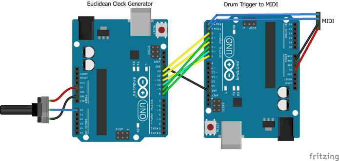
Experiment 1: Arduino to Arduino to MIDI

I could add MIDI functionality to my Euclidean clock generator, but instead opted to build a TRIGGER to MIDI converter using a second Arduino. This has several digital inputs setup to receive TRIGGER pulses and on reception will send out a preconfigured MIDI message.

The configuration is such that a NoteOn is sent for a specific drum on MIDI channel 10 which is typically used for percussion. Which drum corresponds to which input is configurable in the code.

Full details of this so far can be found here: Arduino Drum Trigger to MIDI. This is how I connected them up and it seems to work pretty well.

Arduino to GATE or TRIGGER Output

Here I’m setting up the board to be able to drive an external device.

As always, the standard warning applies – use second hand or disposable equipment for experiments. I am not responsible for damage to expensive instruments. Assess what I’m doing, decide for yourself how it will affect your equipment and then use at your own risk.

I’ve followed the design from HAGIWO’s GATE sequencer, which is detailed in full here: https://note.com/solder_state/n/n17c69afd484d

This recommends the following:

  • All outputs clamped to the Arduino’s 5V and GND using BAT43 Schotky diodes.
  • 470Ω resistor on the output to set an output impedance.

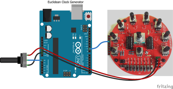
I’m wanting to plug this into my Korg Volca Sync In.

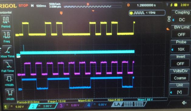
With an oscilloscope I examined the Sync Out signal and confirmed that it is a 5V pulse of 15mS. As I’m only plugging a 5V Arduino into the 5V accepting Korg, I’ve not bothered with the clamping diodes for my simple experiments, but if I build this up into a PCB then I’ll probably add them in to make it a little more universal.

The TRS jack is wired to be compatible with the Korg Volca Sync In port – i.e. using just the tip and shield. A stereo or mono 3.5mm jack to jack cable (as comes supplied with a Volca) can then be used to connect it up.

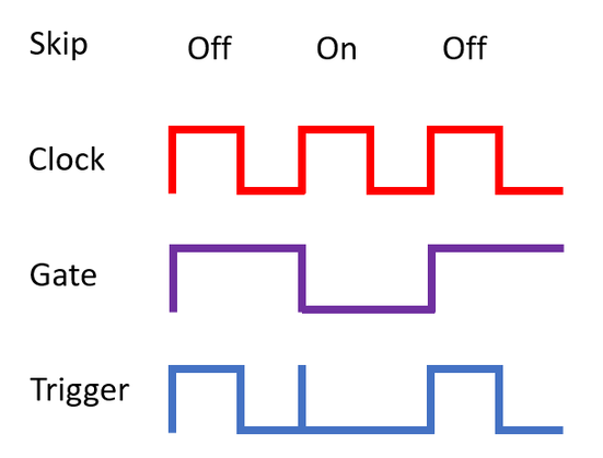
The blue jumper wire can be used to select which of the Euclidean clock outputs to use.

The code is built for TRIGGER mode, so each output is a single 10mS pulse. This is shorter than that produced by the Volcas but generally seems to work.

When first connected or when the tempo is changed I sometimes hear some spurious or irregular triggering, but once it has settled down it seems to work fine for my Volca Keys, Volca Modular, and Volca FM2.

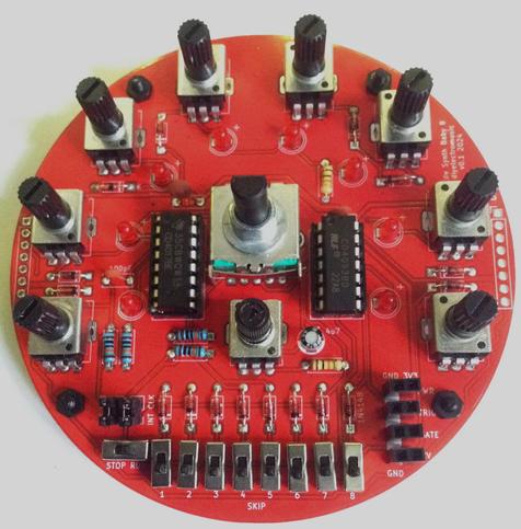
Arduino to ESP32 Synth Thing Baby8

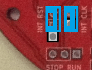
The “Baby8” CV Step Sequencer has an option to be driven by an external clock. If the INT_CLK jumper is removed then it will trigger off whatever is plugged into the CLK header pin (third down from the top of the header).

This means that, assuming the Baby8 is powered off 5V, then any of the Arduino GPIO clock outputs (D8-D13) can be directly connected as shown below.

This is directly connecting the Arduino’s GPIO OUTPUT pins (the clock) to the Baby 8’s 4017 timer CLK pin. As in general terms directly connecting an OUTPUT to an INPUT is deemed an ok thing to do (INPUTs are high impedance as I understand things), i.e. the output of a microcontroller, 555 timer, or NAND oscillator and so on are often set up to drive the CLK pin directly, then connecting it directly to an Arduino GPIO OUTPUT should be fine.

It is also possible to drive the actual Educational DIY Synth Thing itself as it includes 5V tolerant GATE and TRIGGER inputs, but having a regular clock pulse with no pitch CV information is somewhat limited.

But using the Baby8 as shown above with the Synth Thing too should work fine, although if the Baby 8 is powered off 5V then the top of the potentiometer’s range will be slightly too high for the Synth Thing which will top-out at around 3V3. It won’t damage the Synth Thing as the CV inputs are clamped to the 0 and 3V3 power rails.

Closing Thoughts

Naturally getting the logic signal doing the right thing on a GPIO port is only part of the equation. That is only useful if it is able to control something else.

This post looked at some options, from the hacky “quick and dirty” versions through to what ought to be done to do things properly.

I’m still chewing over the idea of some kind of trigger shield or similar PCB.

Kevin

https://diyelectromusic.com/2024/10/07/arduino-euclidean-gate-sequencer-part-2/

#arduinoUno #baby8 #euclidean #gate #midi #stepSequence #synthThing

Arduino Euclidean Gate Sequencer

I’ve always liked the idea of mathematics, algorithms and their application to music, so a Euclidean Sequencer has been on my list of things “to do” for a while. This is my take o…

Simple DIY Electronic Music Projects

For today's pointless MIDI controller, I get my Baby 8 sequencer clocked up to 31250 Hz and use the GATE signal to send MIDI...

https://diyelectromusic.com/2024/09/10/baby8-discrete-logic-midi/

#SynthDIY #Baby8 #DontAskWhy

“Baby8” Discrete Logic MIDI

I’ve wanted to create a non-microcontroller, discrete logic MIDI circuit for some time. I thought it would be interesting to have a few chips that could generate a specific sequence of bytes …

Simple DIY Electronic Music Projects

I’ve wanted to create a non-microcontroller, discrete logic MIDI circuit for some time. I thought it would be interesting to have a few chips that could generate a specific sequence of bytes corresponding to a MIDI message. Note: I’m still talking individual chips here, not just gates and definitely not individual transistors, so perhaps “discrete logic” is a bit of a stretch…

I’ve toyed with various ideas, but not actually properly experimented with anything, but the use of 4017 counters was always there as a possibility.

People have wound up the clocks on a CV step sequencer like these to audio frequencies and created a simple wavetable oscillator.

So seeing as I have a number of “Baby8” CV Step Sequencer PCBs that I’ve just reworked, that will only really work in cascade mode – and seeing as each has 8 switches that control the level of the output GATE signal I thought I would wind the clock up even further and see if I could get it to generate MIDI.

Just don’t ask why.

https://makertube.net/w/oQtoQ4Dgx3rcfBugzr6cyu

Warning! I strongly recommend using old or second hand equipment for your experiments.  I am not responsible for any damage to expensive instruments!

If you are new to electronics, see the Getting Started pages.

Parts list

  • 3x 4017 decade counters.
  • 1x 4093 quad NAND gate (or a dual INVERTER of some sort).
  • 3x failed “Baby8” CV Step Sequencer PCBs (!) with the following:
    • 27x pcb mount SPDT slider switches (2.54mm pitch).
    • 24x 1N4018 small signal diodes.
    • 12x 100K resistors.
    • 3x 100nF capacitors.
    • 3x 100pF capacitors.
    • 3x 8-way right angle pin headers.
    • 3x 8-way right angle pin header sockets.
  • 31250Hz clock signal, e.g.:
    • 1x NAND gate from the 4093.
    • 1x 300R resistor (1% accuracy).
    • 1x 33nF capacitor.
  • 2x 220R resistors.
  • 1x 10K resistor.
  • 1x 5 pin MIDI DIN socket.
  • Solderless breadboard and jumper wires.

The Circuit

I’m not going to go through the core circuit, as the whole point is to reuse the V1 PCBs from my “Baby8” CV Step Sequencer. I only need to use them as a GATE sequencer – no pitch (CV) or trigger is required, so I can ignore the pots, LEDs, the NAND circuitry, and in most cases the clock too.

I also don’t actually need the rotary switch to select the number of steps – I’m going to be fixing it at 8. I could solder in a clock on one of the boards, but the component values would need changing to give me a steady 31250 Hz clock. I’ve opted to use the same circuit but externally on breadboard to achieve this.

Here is the part of the Baby8 schematic I’m actually using.

To generate the clock, I put some values in an online Schmitt trigger oscillator calculator and with some trial and error came up with the use of a 330R resistor and 68nF capacitor for my 31,250 Hz oscillator. But in practice it turns out that 300R and 33nF is much better for what I need. I don’t know where the discrepancy lies – my circuit or the calculator, but with these values I have a good enough (for a couple of bytes) MIDI clock.

The MIDI OUT circuit could possibly have been driven directly off the GATE signal but seeing as I have some inverters kicking around (well, actually several NAND gates from my 4093) I thought I’d buffer the signal and then send it to a standard MIDI OUT circuit.

I’ve only used one inverter, so the MIDI signal will be the inverse of the GATE driving it.

During use, I found I had to pull the GATE signal to GND via a 10K resistor to keep it effective, so again that backs up the idea of using a buffer for the MIDI side to me to keep the two parts independent.

Here is the rest of the schematic with the extras I require:

The whole thing is powered directly from a 5A power supply (in my case actually a DIY circuit using a L7805 – a spare from my MIDI Matrix Patch Bay).

Basic Functionality

The general idea is to have three of these boards cascaded. MIDI consists of several 8-bit values per message, but each of the 8-bits is also accompanied by a START and STOP bit. This means a typical three-byte message (i.e. most of them) consists of 30 bits and a two-byte message (e.g. Program Change) is 20 bits.

I’ve opted to implement something that can generate two-byte, Program Change messages using the 8 switches on three Baby 8s and hooking that up to the GATE signal. The switches will determine if the signal is HIGH or LOW for that stage in the sequence which will be clocked at the MIDI baud rate of 31,250 Hz.

The Baby 8’s will need to start, cascade through an entire sequence of 24 steps (to cover the required 20 bits), and then stop. To do this I’m going to use the “RST return” feature of my PCBs and the RUN switch on the first Baby 8.

Once everything is wired up to the external clock and MIDI OUT circuit, the basic sequence will be as follows. Note I have to power OFF if this is the first use to ensure everything starts in the right place. Further uses do not require a power cycle.

  • Set RUN to STOP on the first Baby 8. It will always be left on RUN on the other two.
  • Power ON if this is the first use.
  • Set the byte values to be sent via the switches.
  • Press the RESET button which temporarily completes the RST chain and ensures the sequencer cycles round to the first step, outputs that GATE value which it will hold and then halts.
  • Set RUN to RUN which then runs through all 24 steps setting the GATE level according to the switch settings.
  • Repeat sequence from the beginning to send further messages.

Assembly and Build

I don’t need to build complete Baby 8 boards – as already indicated I only really want the counter and GATE outputs. These are the sections of the V1 PCB I need to be populated:

As I’m not using the rotary switch, and all the components I’m adding still leave me the option of populating the rest of the components at some point in the future to restore the full (albeit with issues) “Baby 8” functionality, I’ve used the “fishing line trick” to add a non-soldered link between the switch’s step #8 and the return (as indicated in cyan above).

Note that a jumper is required on the last Baby 8 to route the RST signal back through the boards to connect to a manual RESET switch.

Generating MIDI from Discrete Logic

In order to produce a MIDI Program Change message, the following sequence of bytes is required.

MIDI Msg = CMD + DATA
0xCn 0xdd
!! ++--- 7 bit data byte for program number (1..128 = 0x00..0x7F)
!+-------- MIDI channel (1..16 = 0x0..0xF)
+--------- MIDI Program Change command (0xC)

So for MIDI channel 1, the sequence, including START (S) and STOP (E) bits, will be as follows. Note MIDI has the least significant bit sent first, just after the START bit, so reading from left to right is the sequence in which the bits are sent too – time flows to the right (just like an oscilloscope trace).

0xC0 0x04 -> Program Change to voice 5

0 0000 0011 1 0 0010 0000 1
S Ch1 PC E S Data=4 E

This requires the switches set as follows:

HLLL LLLL HHHL LLLH LLLH HHHH
+------- STOP and remain HIGH to finish
++++-+++-------- 7 bits of data to encode 0x04
+----------------- START
+------------------ STOP
++ ++------------------- 4 bit command 0011 = 0xC (PC)
++ ++------------------------ 4 bit channel 0000 = 0x0 (Ch 1)
+----------------------------- START
+------------------------------ Preamble starts HIGH

Due to the use of the inverter as a MIDI OUT buffer, a H is generated from the GATE being LOW – i.e. having a step skipped (switch down).

In order to ensure I get a good START bit, the first switch (which is the “hold” step until the RUN is started) is set to generate and therefore hold a H level.

The program number to be set is chosen by encoding a number between 0 and 127 (corresponding to programs 1 to 128) backwards (the step sequence is also left to right) on the appropriate 7 switches – four on the second Baby 8 and three on the last.

Here are some traces of the boards in action. Both traces show selecting voice 5 (sending byte 0x04 as data).

The first is a trace from my Arduino MIDI Logic Analyser, which also gives an estimate of the baud rate in use. I had to modify it slightly to cope with two-byte messages – it was only dealing with three-byte messages before. I’ll update the code and message handling one day.

We can see that the baud rate is still a little high compared to what is required, but it seems close enough for just a two-byte message.

And here is an oscilloscope trace of the clock signal (blue) and the MIDI OUT signal (yellow) for the same message.

The first drop is the START bit. The two highs are the end of the PC byte and the STOP bit. Then there is another START bit and then binary 0010 – which is 4 when encoded LSbit first (on the left) followed by more zeros until the final high STOP bit and a few trailing highs.

Conclusion

I’ve wanted to do something like this for a while now so actually really quite enjoyed this somewhat pointless activity. Of course, using PCBs like these is massive overkill and the utility of the result is very questionable.

The video shows me selecting different patches on a MiniDexed. You can just about see the voice name change on the display, but hopefully you hear the difference going from Brass 1 to Strings 1, Strings 3, Strings 2 and back to Brass 1 again.

But the V1 PCBs were sitting on my bench, and for the sake of soldering on a few cheap components provided an easy way to test the idea.

And I’ve not soldered anything on that means I couldn’t turn these back into full (but limited) Baby 8 sequencers if I wanted.

So I’d say this is a win. But as I say, just don’t ask me why.

Kevin

https://diyelectromusic.com/2024/09/10/baby8-discrete-logic-midi/

#8 #baby8 #midi #programChange #sequencer

“Baby8” CV Step Sequencer – Part 2 – PCB Design

This is a PCB design for a full “Baby 8” style sequencer based on the ideas presented in “Baby8” CV Step Sequencer – Part 1. Key features I’m after: Fully analog CV, gate and…

Simple DIY Electronic Music Projects

"Baby8" Discrete Logic MIDI (ish)

https://makertube.net/w/oQtoQ4Dgx3rcfBugzr6cyu

"Baby8" Discrete Logic MIDI (ish)

PeerTube

Well it isn't without its quirks, but in essence the cascade works :)

The video shows two of my Baby 8 style sequencers linked together to give a 16 step sequence.

https://makertube.net/w/iD2K8ett5KDeSSi6maHtox

#SynthDIY #Baby8 #SynthThing

Baby 8 CV Sequencer Cascade

PeerTube

I've now published my design, build and usage notes for my "Baby 8" style CV step sequencer for use with my ESP32 Educational Synth Thing.

Full details can be found linked off the following, which includes a short video of it in use: https://diyelectromusic.com/2024/09/01/baby8-cv-step-sequencer-part-4-in-use/

Kevin

#SynthDIY #Baby8 #SynthThing

“Baby8” CV Step Sequencer – Part 4 – In Use

These are the usage notes for my “Baby 8” style sequencer based on the ideas presented in “Baby8” CV Step Sequencer – Part 1 and using the PCB I’ve described in part 2 and pa…

Simple DIY Electronic Music Projects

These are the usage notes for my “Baby 8” style sequencer based on the ideas presented in “Baby8” CV Step Sequencer – Part 1 and using the PCB I’ve described in part 2 and part 3.

  • Part 1 – This post with the introductory design information.
  • Part 2 – The design for a PCB based on the principles in the first post.
  • Part 3 – The build and test notes for the PCB.
  • Part 4 – Usage notes for the PCB and how to use it with the Educational Synth Thing.

The video shows it connected up to my Educational DIY Synth Thing.

https://makertube.net/w/vP4orcyfKqkRYG8qn5Z9p5

Warning! I strongly recommend using old or second hand equipment for your experiments.  I am not responsible for any damage to expensive instruments!

If you are new to electronics, see the Getting Started pages.

Basic Single Use

The jumpers must be set as follows for single-use:

The key controls and principles of operation are as follows:

  • Tempo is set by the central potentiometer.
  • The number of steps is set using the rotary switch to between 1 and 8.
  • The pitch of each step is set by each of the 8 potentiometers to between 0V (off) and almost the power level of the supply (3V3 or 5V).
  • Each step can be skipped, but this only skips generating the GATE and TRIGGER signals. The CVs are still updated.
  • The TRIGGER signal has a pulse width that matches the current clock, so will be longer for slower tempos.
  • If all steps are active then the GATE signal will be on constantly.
  • CVs are constantly generated for all steps regardless of the use of TRIGGER or GATE.
  • The “run” switch can be used to pause the clock.

The following trace shows the interactions between the TRIGGER (yellow), reset signal (blue), clock (magenta) and GATE (darker blue) for a switch pattern where steps 2, 5, and 6 are being skipped.

Note that pattern has just started to repeat with the next step 1 and the skipped step 2 just on the screen.

Cascading Units

There are two 8-way headers on the boards with pins as follows:

This means that it should be possible to plug the boards directly into each other, change the jumper settings and have the boards work in a cascade mode.

The final E_RST_OUT must be routed back to the first E_RST_IN. This can be done with a long jumper wire connecting the two “EXT” pins.

But there is also a “RTN” header pin which has no other purpose than to provide an internal return path back through each board, so one only has to jumper these two signals together at each end to make the return link, as shown below.

The “RST” jumper must be removed to enable cascade mode (note: this is labelled “INT RST” on V1 of the board, but “EXT RST INT” on V2).

Photo on the right shows the jumper set for external cascade operation. Photo on the left shows the jumper set for internal operation.

Reducing the Steps

The two step selection switches will still work, but note that pots for the resetting step will still be active when cascading. This means that if the pot is turned up higher than any of the other units steps then that voltage will dominate the CV output.

It is therefore important that the pots for any skipped steps are turned right down to zero.

Note: skipping steps works as before – i.e. it results in no GATE or TRIGGER signal but does not skip the CV output itself.

Cascading Clocks

When cascading the sequencers, all but one should have their clocks disabled. This means removing the “INT CLK” jumper. The board that retains its jumper will be the master clock for all the boards.

External Clocks

In principle it would be possible to disable the clock on all modules and have then driven by a completely external clock signal via the external IN CLK signal. Similarly in principle it would be possible to hook up the CLK signal of the external OUT header to another device.

Warning: This is not recommended as there is no protection circuitry for completely external signal inputs such as a clock or to drive completely external devices.

Cascading Two Units

https://makertube.net/w/iD2K8ett5KDeSSi6maHtox

Use with the EduModSynthThing

A key reason for building this was to be able to use it with my Educational DIY Synth Thing. The following diagram shows how to do that for a module in single mode.

The key connections are:

  • GND and 3V3 to the Baby 8 GND/3V3 power input.
  • Baby 8 CV OUT to one of the VCO pitch inputs.
  • Then there are some options:
    • Ignore TRIGGER and GATE on the Baby 8 and just connect 3V3 to the VCO CV.
    • Connect TRIGGER and GATE on the Baby 8 to one of the EGs.
    • Connect GATE on the Baby 8 to one of the EGs and then patch TRIGGER and GATE together.
    • Connect TRIGGER on the Baby 8 to one of the EGs and then patch TRIGGER and GATE together.

TRIGGER will determine when the envelope generator starts (or restarts) the envelope. GATE determines when the release phase will start – i.e. when the GATE is released.

Just using the GATE as both gate and trigger means that a new sound will only be triggered after a skipped step. Just using the TRIGGER as both gate and trigger will mean that each note lasts half as long as the clock as each.

A key consideration is that the Baby 8 GATE will never be off if no steps are skipped, so the envelope will never start a release phase.

Another consideration is that if the release takes longer than each step, then subsequent steps, even if skipped, will still sound as the CVs are continually generated.

Closing Thoughts

It takes a bit of thinking about to realise how the GATE and TRIGGER signals interact with the envelope generator of the synth. But that is kind of the point – it is meant to allow simple experimentation to help understand what is going on.

In short, I’m really pleased with how this has come out and once I realised the CV issue with skipped steps, the cascading seems to work fine too.

Kevin

https://diyelectromusic.com/2024/09/01/baby8-cv-step-sequencer-part-4-in-use/

#baby8 #pcb #sequencer #synthThing

“Baby8” CV Step Sequencer – Part 1

A common early project for anyone starting to play around with analog synthesis is a “Baby8” step sequencer. There are many designs out there on the Internet and many ready-designed kit…

Simple DIY Electronic Music Projects

Baby 8 CV Sequencer for the ESP32 EduSynthThing

https://makertube.net/w/vP4orcyfKqkRYG8qn5Z9p5

Baby 8 CV Sequencer for the ESP32 EduSynthThing

PeerTube

Here are the build notes for my “Baby8” CV Step Sequencer PCB Design.

  • Part 1 – This post with the introductory design information.
  • Part 2 – The design for a PCB based on the principles in the first post.
  • Part 3 – The build and test notes for the PCB.
  • Part 4 – Usage notes for the PCB and how to use it with the Educational Synth Thing.

Warning! I strongly recommend using old or second hand equipment for your experiments.  I am not responsible for any damage to expensive instruments!

If you are new to electronics, see the Getting Started pages.

Bill of Materials

  • “Baby 8” CV Step Sequencer PCB (GitHub link below)
  • 1x CD4017 decade counter.
  • 1x CD4093 quad Schmitt trigger NAND gate.
  • 16x 1N4198 small signal diode (or equivalent).
  • 8x 3mm or 5mm LEDs.
  • 4x 100KΩ resistors.
  • 3x 10KΩ resistors.
  • 1x 500KΩ potentiometer (RV09 style – see photos and PCB for footprint).
  • 8x 10KΩ potentiometer (as above).
  • 1x 100pF ceramic capacitor.
  • 2x 100nF ceramic capacitors.
  • 1x 100nF ceramic capacitor or 1uF electrolytic (see errata).
  • 1x 4.7uF electrolytic capacitor.
  • 1x 8-way rotary switch (see photos and footprint and below for details).
  • 9x SPDT slider switch, pcb mounting, 2.54mm pitch.
  • Jumper pin headers and jumpers.
  • Optional: 1x 16-way DIP socket; 1x 14-way DIP socket.
  • Optional: 4x 2-way jumper header sockets.
  • Optional: 1x 8-way right angle header socket.
  • Optional: 1x 8-way right angle header pins.

My 8-way rotary switch was called “RS17 Band Rotary Switch 1 Pole 8 Position” on an overseas marketplace. I had to design the footprint myself (see the design notes) so be sure to compare the measurements. The key dimensions being:

Build Steps

Taking a typical “low to high” soldering approach, this is the suggested order of assembly:

  • All resistors and diodes.
  • DIP sockets (if used).
  • Disc capacitors.
  • LEDs (if mounting flush).
  • Electrolytic capacitor(s).
  • Slider switches (if mounting flush).
  • Jumper headers and pins.
  • Potentiometers.
  • Rotary switch.

Here are some build photos of the first version of the PCB. The second version fixes a few issues, but the build process is largely the same. Note there is one errata for the additional capacitor added in the second version of the board (see below).

Note: If a front panel is to be used then it might not be possible to use IC sockets as that would leave the ICs too high off the PCB.

The LEDs and switches can be mounted flush with the PCB, but if a panel is to be used they would probably need to be mounted at a suitable height to be flush with the panel.

The final stage is to mount the potentiometers and the rotary switch. It is recommended that the 500KΩ (marked “B5 04” probably, compared to “B1 03” for the 10KΩ pots) is fitted first to ensure it doesn’t get confused with the others.

When it comes to adding headers, there are a range of options. I’ve opted for the use of right-angled, connecting headers as shown below.

Note that the pin headers are initially soldered in the “wrong” way round to ensure that the pins will be at the same level as the socket when I connect two modules together. I left the plastic shroud on whilst soldering but then removed it.

The board was then mounted on four M2.5 spacers (nuts and standoffs).

Testing

I recommend performing the general tests described here: PCBs.

This PCB can run off 5V or 3V3 (and to be honest, any supported voltage of the 4017 and 4093 being used).

Basic checks should be performed in stand-alone mode, i.e. the two jumpers are linked as to enable the internal clock and connect the CLKINH/CKEN signal into the reset chain (assuming the second version of the board):

Then the following can be checked:

  • Step switch reduces the number of steps appropriately.
  • The tempo switch adjusts the speed of the sequence.
  • The full output CV should be close to the VCC level used (i.e. 3V3 or 5V).
  • The pots should adjust the CVs for each step.
  • The GATE should be HIGH for every step that is enabled via the switches and LOW for any that are skipped. Note: there are no gaps in the GATE signal if all switches are enabled.
  • The TRIGGER signal should be momentarily HIGH for every step that is enabled via the switches.

PCB Errata

There were a number of issues with the first version of the PCB, but the second, currently published version, should have fixed them.

However – the additional resistor and capacitor added to smooth out the trigger is stated as a 0.1uF ceramic capacitor in the schematic and on the silkscreen. Further testing appears to show that a 1uF electrolytic is more effective.

This has to be oriented as shown below, with the -ve (stripe) side towards the resistor. Care must be taken to ensure that the pot and rotary switch will still fit on the PCB around the capacitor.

Enhancements:

  • None

Find it on GitHub here.

V1 PCB Patch and Workaround

There were three issues with V1 of the PCB:

  • CLKINH/CKEN is not wired correctly for stand-alone (non-cascading) use.
  • There are spurious triggers when steps are skipped.
  • The pots are wired backwards. Again. Sigh.

The first two have patches and workarounds. I just had to live with the pots.

The main issue with the CLKINH/CKEN signal is that for use as a standalone module, the CLKINH/CKEN pin really needs to be left pulled LOW to GND. But as designed in V1 it will receive a pulse along with the RST pin when the counter resets. When cascading to a second counter this is correct and desired behaviour. When fed back into the same counter it causes issues.

There are two possible workarounds, a simpler one and a more complex one. Both require cutting tracks on the PCB.

The Simpler CLKINH Workaround

This involves using the external RST connections on the IN and OUT headers. The external RST OUT is used to feed to RST signal back into the external RST IN rather than having it routed through the PCB. This means that the CKEN signal can be left pulled LOW to GND and not be involved in the RST itself.

There are two cuts required on the underside of the board as shown below.

In addition to the PCB cut traces it requires the following:

  • The “INT RST” jumper must be removed (highlighted in yellow above, shown from the underside of the board).
  • The OUT external RST signal must be connected to the IN external RST signal.

The RST connection can be done either with a long jumper wire from the OUT (on the right hand side) to the IN connector (on the left hand side); or by connecting the external RST signal jumpers to the adjacent “RTN” pins, which were added for exactly this reason, albeit for use when cascading modules. This second options is illustrated by the two green connections in the above photo on the two opposite sides of the board.

Note: To re-cascade a patched PCB will require getting the output RST signal from the OUT header back over to the CLKINH/CKEN line via the internal RST jumper (which will be removed anyway for cascade).

The Complex, but more Complete, CLKINH Workaround

In order to preserve the configurability of the module, it is possible with some care to turn the 2-way “INT RST” jumper header into the 3-way jumper as per the updated schematic in the design.

This requires drilling an additional hole in the PCB and adding some patch wires in addition to cutting traces. This is illustrated below.

Here are the steps required:

  • Drill an additional through-hole to make the “INT RST” jumper a three-way jumper. The hole should be just below the existing header, keeping the 2.54mm standard spacing. The other holes are 0.8mm diameter.
  • Any copper trace from the GND zones on both sides of the board around the new hole must be removed to prevent shorting to GND.
  • Cut the same two traces as for the “simple workaround” – shown in blue on the underside of the board on the left-hand diagram.
  • Cut one more trace on the topside of the board. This is the trace between the “INT RST” jumper and the left-most, vertically oriented 100K resistor – again as shown in blue on the right-hand diagram.
  • Solder two jumper wires (shown in green on the right-hand diagram): one between the rotary switch and the new centre of the 3-way jumper; and one from the right-most (as seen from below) 100K resistor to the new pin of the 3-way jumper.
  • Once complete, the new 3-way jumper can be used to switch between “internal” mode (with the top two pins jumpered) and “external” mode (with the bottom two pins jumpered).

    Preventing Spurious Triggers

    The key here is to add a small RC circuit between the CLK and the trigger circuitry as shown in the updated schematic:

    On V1 of the board there is a track that connects the 4017 to the 4093 using a via. This can be cut (blue arrow below) and a 10K resistor used instead between pin 6 of the 4093 and the 100K resistor connected to pin14 of the 4017 (green arrows below).

    Then the 4093 side of the resistor can be connected to GND using the 100nF capacitor (other green arrow).

    Closing Thoughts

    You think by now that I’d get the pins of the potentiometers the correct way round – hey ho. That isn’t a major issue. The other two issues come from being able to practically try out the board and issues like this aren’t unusual really in a prototype.

    Taken together all three made it worth getting a V2 board built.

    I would definitely like to make a panel for this module, but am not sure about the component heights at the moment. The switches do look like they might be an issue as I don’t think the legs are long enough.

    Kevin

    https://diyelectromusic.com/2024/09/01/baby8-cv-step-sequencer-part-3-pcb-build-guide/

    #baby8 #pcb #sequencer

    “Baby8” CV Step Sequencer – Part 2 – PCB Design

    This is a PCB design for a full “Baby 8” style sequencer based on the ideas presented in “Baby8” CV Step Sequencer – Part 1. Key features I’m after: Fully analog CV, gate and…

    Simple DIY Electronic Music Projects

    This is a PCB design for a full “Baby 8” style sequencer based on the ideas presented in “Baby8” CV Step Sequencer – Part 1.

    • Part 1 – This post with the introductory design information.
    • Part 2 – The design for a PCB based on the principles in the first post.
    • Part 3 – The build and test notes for the PCB.
    • Part 4 – Usage notes for the PCB and how to use it with the Educational Synth Thing.

    Key features I’m after:

    • Fully analog CV, gate and trigger outputs.
    • Configurable number of steps up to 8.
    • Internal, adjustable clock source.
    • Cascadable.
    • Fully compatible with my Educational DIY Synth Thing.
    • Arranged in a circle.

    Warning! I strongly recommend using old or second hand equipment for your experiments.  I am not responsible for any damage to expensive instruments!

    If you are new to electronics, see the Getting Started pages.

    The Circuit

    This has taken the oscillator and cascading 4017 counter design from part 1 and added the CV and gate sequencer output stages. The main design is largely based on several designs found around the Internet.

    The CV signal is a simple sum, via a diode, of a potentiometer output from the counter output stages. Each output line also has a LED connected via a single 10K resistor to GND. As each LED will only be on one at a time in turn, I’ve just used a single common resistor.

    The gate signal goes via a switch and another diode. The switch can be used to “skip” a step. Note this doesn’t completely skip the step rather just stops the gate being active for that step. It is also not a full “mute” switch as the CV will still be generated.

    A trigger output is also required. This is created by taking the gate signal and using a couple of the NAND gates from the 4093 to only output a signal when both the gate and the clock is active. As the clock has a 50% duty cycle – i.e. is high for half a period and low for half a period – this creates a pulse for every clock tick that the gate is active. Two NAND gates are required as one acts as an inverter to create a “active HIGH” pulse.

    One common problem with generating triggers from gates with a Baby 8 is that the gate won’t be turned off until the next clock cycle. This means there is a slight overlap where the next clock is high but the gate is about to go low. This will cause a spurious trigger for any steps where the “skip” switch is on. This is illustrated below for three steps with skip on for the second step.

    One solution is a simple RC circuit that causes a very small delay to the clock signal as it enters the trigger circuit. My initial experiments appeared to show that a 10K resistor and 100nF capacitor was enough to remove the spurious trigger, so that is what I put in the schematic and the second version of the PCB. Subsequent experiments appeared to show that this wasn’t enough so in further builds I’ve replaced the 100nF capacitor (C5 in the schematic) with a 1uF capacitor instead.

    In terms of cascading sequencers, there is a “in” and “out” header which contains all the required signals. The headers also include a “return” signal which can be used to link the last sequencer in a chain back to the first without lots of extra wires.

    When cascading modules the internal clock needs to be disabled on all but one module; and the internal resets must be disabled on all modules. This is done via jumpers.

    One thing I hadn’t picked up on in my earlier experiments is that when designing the circuitry for a cascading sequencer it is useful to be able to tie the CLKINH (or CLKEN) back to GND when in single-use mode. Otherwise there is a pulse on CLKINH at the same time as a reset and odd things can happen, including missing step 1. As there is already a pull-down resistor on the CLKINH line, it is simply a case of being able to unlink this line from the rest of the RST circuitry.

    Consequently the RST jumper selects between connecting RST OUT to RST IN (when in single use mode) to hooking CLKINH into the RST sequence (when in cascading mode).

    The output electrical and physical arrangements are designed to match what I need for my Educational DIY Synth Thing. They are not designed as such for use with other systems – i.e. there is little protection, buffering, or adjustment of signals going on.

    The whole thing can be powered from either the 3V3 or 5V line of the Synth Thing and the output range for CV and gate/trigger will scale accordingly.

    However it is worth noting that as the output is passing through a diode there will be a slight non-linearity in response – there won’t be an output until the voltage is larger than the forward voltage of the diode, and there will be a bit of a voltage drop too. This will be more pronounced when running at 3V3 than 5V but I’m not anticipating it being a major issue for what I want to do.

    PCB Design

    Probably the most “fun” part of this was getting the positioning right for the circular placement! In the end I broke out a spreadsheet that took the angular separation and outputted the values I needed, allowing for things like the offset of the “origin” point for a component within its footprint in KiCAD compared to where I wanted it centering. For example, I wanted the hole/circle of a pot to be the centre-point of the placement, but those pot footprints have an origin at pin 1 which is both below and 2.54mm offset from the centre.

    Fun facts: the plotting function allows a quick sense-check. The SIN() and COS() functions work fine as long as you remember to RADIANS() any value in degrees 🙂

    I was able to repeat the same process for the LEDs. These were slightly easier as the origin offset was just half a standard header space away – i.e. 2.54mm/2 = 1.27mm.

    I didn’t have a footprint for the multi-way switch, so I had to go back to the provided spec from my purchase and make a footprint from that. One quirk is that the mounting holes are slightly off-centre. Also two of the end pins are both wired as the common switch element.

    Originally I was going to have the knob for the switch in the centre of the board, but I couldn’t quite make it fit. But the two controls are pretty much in the centre.

    I’ve used standard 2.54mm spacing for the switches. This matches the cheap slider switches I have.

    There are three sets of header pins – an in and out header for the cascade function, and a complete set of control headers for the CV, gate and trigger outputs and power input. There are two jumpers that switch over the clock and reset lines to allow them to be cascaded.

    Closing Thoughts

    The first issue board had several problems, which were all patchable, but have made me decide to do a second issue:

    • There was the problem with the CLKINH/CKEN pin. I was just going on what the circuits that have been published elsewhere seem to be saying and none seem to talk about this issue. I’m still not entirely sure why it hasn’t worked, but I think it is some interaction between CKEN temporarily going HIGH in the reset condition causing the counter to miss a clock pulse somehow. Anyway having the jumper to delink CLKINH works fine.
    • My initial version had the spurious triggering issue, so the second version added the RC circuit.
    • And annoying, I’d wired all the pots the wrong way round! I can’t believe I’m still managing to get that wrong in designs! 🙂

    Putting all that aside, I think I’ve arranged things so that it ought to be possible to design a panel and case for this board to match the other devices I have, but I’m not sure about the heights of components. The LEDs should be ok to be extended but the switches are likely to prove problematic.

    I have included mounting holes though so an “open top” case is certainly a possibility.

    Kevin

    https://diyelectromusic.com/2024/09/01/baby8-cv-step-sequencer-part-2-pcb-design/

    #baby8 #pcb #sequencer

    “Baby8” CV Step Sequencer – Part 1

    A common early project for anyone starting to play around with analog synthesis is a “Baby8” step sequencer. There are many designs out there on the Internet and many ready-designed kit…

    Simple DIY Electronic Music Projects