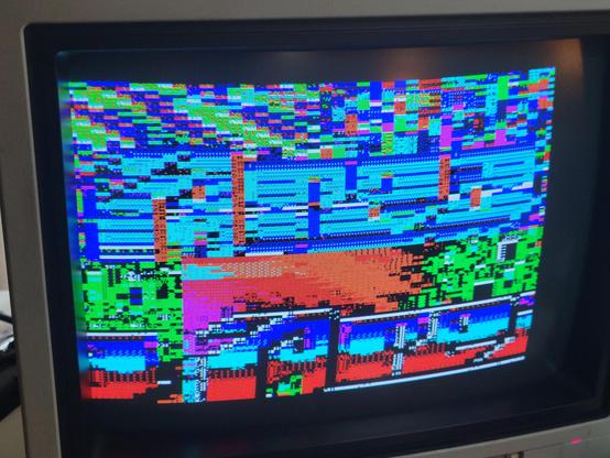
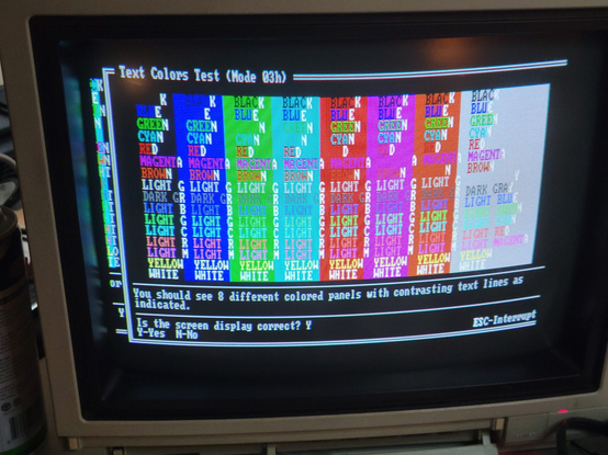
We have a picture. It isn't perfect - there's some flickery bits - I don't know if dot crawl is the right word. Not sure what's going on there.
Driving sync signals with a single image buffer was untenable - it's really difficult to have seamless, continuous DMA on the Pico. Every time you restart DMA there's a discontinuity, and if the thing you're DMA'ing represents every single clock cycle in a video field, inserting extra time messes up your picture.
So separate PIO programs generate hsync and vsync, and we restart our now image-only DMA in vsync, just like the OG Glyphblaster does, which we already know works.
I think the crawling may be that the color output is not perfectly aligned with the dot clock.
I'm starting to think a pico is not the appropriate thing to build a video card with.
all my fun ideas always end up with me concluding i should use an FPGA.
FPGAs are like the crabs of electronics projects. everything wants to turn into an FPGA if you give it enough time.
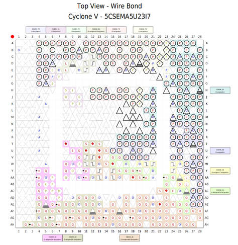
okay this isn't that confusing
for example, these are the snake pins. you can choose from left snakes or right snakes

you know, there's a very good reason NOT to use an FPGA
when you actually use the proper tools for a job, it stops becoming a hack.
you're no longer a hacker, you're some kind of engineer or something. ugh.
Okay, lets see if I can get a 14.31818MHz clock out of this thing.
We have a 50MHz clock source, on a pin called FPGA_CLK1_50.
How do we get 14.31818MHz out of that?
By attaching a PLL to it, hopefully.
module de10_clock_test (
    input  wire FPGA_CLK1_50,
    output wire GPIO_1_0
);

    wire clk_osc;
    wire pll_locked;

    cga_pll pll_inst (
        .refclk   (FPGA_CLK1_50),
        .rst      (1'b0),
        .outclk_0 (clk_osc),
        .locked   (pll_locked)
    );

    assign GPIO_1_0 = clk_osc;
endmodule
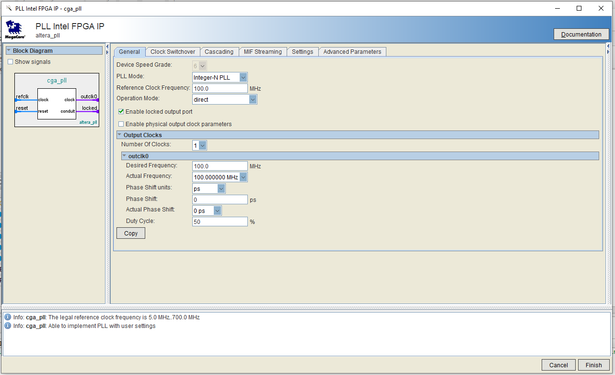
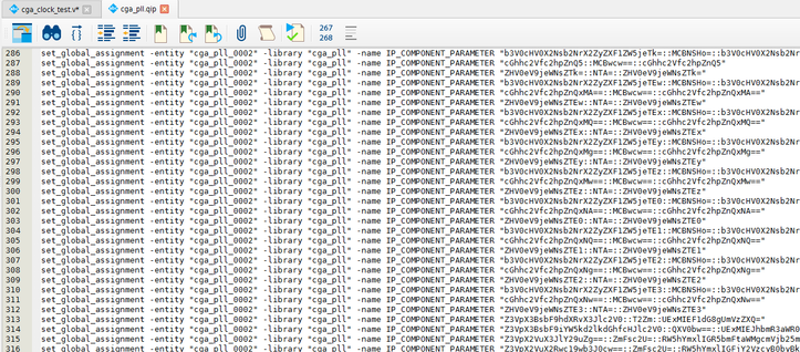
pll_inst is a PLL instantiation. But notice it says nothing about like dividers or anything. We have to go into something confusingly called the IP (Incendiary Pickle) Catalog to actually configure the PLL.
This is far as a I get because doing this causes Quartus to hang.
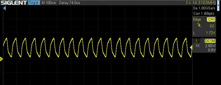
Okay, if I did all this right, i should have a 14.31818MHz clock on GPIO pin 1.
Let's find out! To the workbench!
Hot damn!
looks just like the Pico clock - maybe it is my probe, lol.
So, the cool thing about FPGAs, is that this clock signal now just ... lives inside the vast and mysterious gate goo within the chip. We connected it to GPIO1, but we can connect it to just about anything, internally or externally, and we can trigger other logic on it.
It's like real legit design shit. It makes the Pico's PIO mode feel like a bit of a toy.
So remember that digital logic simulation I made of the CGA card in Digital?
Digital can export your entire simulation to Verilog.
In theory, I just need to wire up the OSC pin to this 14.31818Mhz PLL clock, and wire the simulation's output pins to some GPIOs, route them out through a 244, and I'll have a picture on screen.
surely it can't be that simple?
that would be a neat party trick but i wouldn't really learn anything and i'm sure the resulting Verilog would be spaghetti.
let's actually build this thing intentionally. Generating a clock was fun but i'm actually going to let the Pico continue to do that, and we'll treat a GPIO on the FPGA as the OSC input pin.
We'll divide it by 8, feed it to my Verilog MC6845 pre-configured for 80-column text mode, and wire up the HSYNC and VSYNC outputs to two more GPIOs.
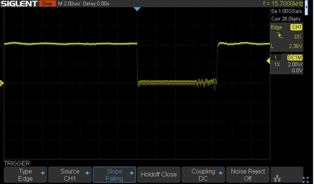
We should get a 15.7kHz HSYNC and a 59.9kHz VSYNC out of that.
This is incredibly cool.
This is a spot-on, 15.7kHz horizontal sync pulse generated the Cyclone V FPGA running my (very simplified) Motorola 6845 Verilog implementation!
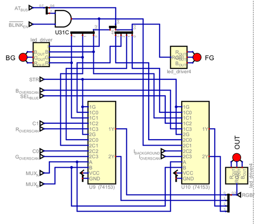
The DE-10 Nano has four user switches. The CGA outputs 4 bit color. Very convenient. Since I don't have any video memory yet, I'm just going to assign each switch to a color component, and AND it with display enable from the 6845. This should give us a well defined display rectangle on screen.
That looks something like this
    wire display_en = crtc_de;

    assign CGA_R = display_en ? SW[0] : 1'b0;
    assign CGA_G = display_en ? SW[1] : 1'b0;
    assign CGA_B = display_en ? SW[2] : 1'b0;
    assign CGA_I = display_en ? SW[3] : 1'b0;
Well, it took me a bit to figure out that the 47pF capacitors right at the D-SUB connector are not optional, specifically on HSYNC. This explains why the RGB2HDMI would sync to things the real monitor wouldn't.
But hey look, FPGA CGA video!
I didn't properly reset the green switch which is why we got cyan instead of blue. lol. But they do all work.
The FPGA is being fed the 14.31818 clock from the Pico to simulate the ISA bus' OSC pin as an input to some future card. I'm going simulate the ISA bus with Picos until I have some idea how I'm going to connect all this business to an actual PC's ISA bus.
It's a bit silly to talk about building an FPGA-based CGA card without mentioning the Graphics Gremlin, by @tubetime
https://github.com/schlae/graphics-gremlin
He's already made such a thing.
I'm interested in writing my own Verilog implementation, and of course I want to stick a Pico 2 W on it so we can stream video to it, but it seems sensible to fork the Gremlin instead of re-inventing the entire wheel.

There are some downsides, apparently this is a somewhat expensive card to build, just looking through forum discussions. But it's been five years, maybe there are better/cheaper FPGA options available today?
The Gremlin uses a Lattice iCE40 HX FPGA that costs about $20. That's not outrageous.
It has 7680 LUTs.
The Cyclone V I'm using has 110,000, but then again this FPGA is massive overkill. It can emulate a Nintendo 64, after all.
A lot has changed in the last 5 years since the Gremlin was specc'd out.
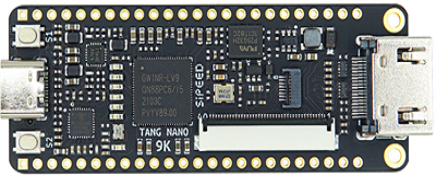
This is a Tang Nano 9k. It's about $22 on AliExpress.
It has 8640 LUTs, onboard SPI flash, and an HDMI port (!)
It could be socketed so you could take it out and use it for something else if you got bored with your ISA GlyphBlaster.
There's even a Tang Nano 20K now that has 8MB (yes MB) of SRAM on-board, and an SD-card reader. It's $45.
That's like your whole ass GlyphBlaster right there, just add bus buffers and a de-9 port.
Turns out the 244 buffer I pulled out of my cheapo amazon special Box o' Components was just bad, or maybe I inadvertently killed it.
In any case, I replaced it with one from the Chameleon and most of my signal issues cleared right up.
Translating my digital simulation into Verilog proceeds slowly. It's nice that I can copy and paste parts of the sim and export them to Verilog in isolation, then it's a a matter of simplifying things and making connections back to the main file.
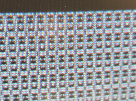
I've got the font ROM in place and the chargen serializer. To test it, I hardcoded the font ROM's upper 8 address, then I AND the serializer output directly with the color switches.
What does that all mean? We have smiley faces!
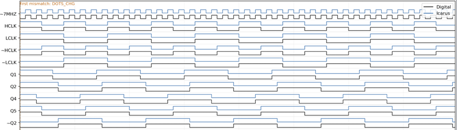
I found a pretty decent way of checking my work against the digital simulation.
We can just run the card in a test harness in iVerilog, and export a CSV of signal states, so we can do a direct comparison against a CSV dumped from Digital.
This is a whole lot easier than using the oscilloscope lol.
It helps not to wire your DRAM address pins backwards.
Still major issues to iron out.
We're getting there. Still have an issue with alignment of glyphs and attributes.
I'm not sure how, since my latch signals for characters and attributes match the simulation. But baffling bugs are the best kind of bugs.
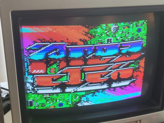
its still kind of weird seeing like, readable text on a monitor, and knowing this isn't IBM or Tseng Labs or Cirrus Logic it's just GloriousCow.
I made a video card?? you can just do that? isn't it illegal?
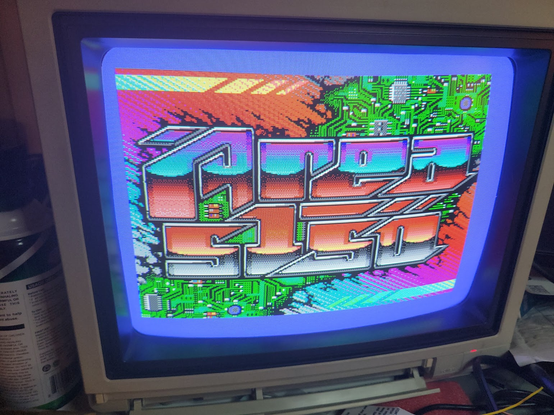
I took a peek at the Verilog source for the Graphics Gremlin and I think I know why it may have trouble with 8088MPH and Area 5150. I'd love to offer a hand at fixing it, but I'm not paying $200 for one from Germany.
Anyone out there have a Graphics Gremlin they'd be willing to loan me for the cause?
Text mode working, with proper glyph/attribute alignment. I had my Johnson Counter wired up wrong.
(That's what she said)
so i have a few reflections on this endeavor so far - I don't want to sound like i'm just bragging, even if I am a little bit.
Making your own FPGA video card may sound like some sort of omega-level nerd activity, but this wasn't fundamentally all that difficult. The CGA is made almost entirely of off-the-shelf 74-series logic chips, a ROM, some DRAMs, the Motorola MC6845, and a delicious sprinkling of resistors and capacitors.
There's probably some stuff you always wanted to learn but maybe the thought scares you a bit. It feels too big.
I bet you, if you can find the time, you'll be looking back before you know it, knowing how to do that thing and wondering what you were scared about.
i might as well show some Verilog, and then people who know what they are doing can make fun of me
the CGA has a ton of flip-flops. like a metric ass-ton of flip-flops. So I made this module for a 74ls174, wich is a 6-bit D-flop with clear.
module ttl_74174 (
    input  wire       clk,
    input  wire       clr_n,
    input  wire [5:0] d,
    output reg  [5:0] q
);

    always @(posedge clk or negedge clr_n) begin
        if (!clr_n) begin
            q <= 6'b000000;
        end else begin
            q <= d;
        end
    end

endmodule
what's a D-type flip-flop you ask? well, the D stands for Deez.
the top bit just defines the input and outputs. you can group things into busses, like we grouped all six of the inputs and outputs into d and q, which each has six wires indicated by [5:0]
i'm still not really sure when to use a reg and when to use a wire.
anyway, a D-type flipflop latches its deez when it is clocked.
so with always @(posedge clk we are saying "do this shit every time the clk input has a rising edge" and we latch q with d via q <= d.
very simple. you didn't even need to go college for this. you're welcome
you could literally just model every single chip like this, and just connect them up the way they are actually connected. that would work. it wouldn't be much fun to read though.
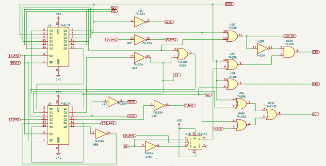
the CGA generates a ton of clocks via something called a Johnson Counter which is just a funny name for people feeding outputs of a flip-flop back into the next inputs of a flip-flop in stages.
this is what happens when you wire up the literal chip connections:
    assign u4_d = {
        u4_q[4],   // 6D
        u4_q[3],   // 5D
        u4_q[2],   // 4D
        u4_q[1],   // 3D
        u4_q[0],   // 2D
        ~u5_q[1]   // 1D
    };

    assign u5_d = {
        ~u5_q[1],            // 6D
        ~u5_q[4],            // 5D
        ~u5_q[3],            // 4D
        u4_q[3] ^ ~u5_q[1],  // 3D
        u5_q[0],             // 2D
        u4_q[5]              // 1D
    };

    ttl_74174 u4 (
        .clk   (clk_14),
        .clr_n (reset_n),
        .d     (u4_d),
        .q     (u4_q)
    );

    ttl_74174 u5 (
        .clk   (clk_14),
        .clr_n (reset_n),
        .d     (u5_d),
        .q     (u5_q)
    );

    assign lclk_n    = u4_q[0];
    assign lclk      = ~lclk_n;
    assign clk_q2_u4 = u4_q[1];
    assign clk_q4    = u4_q[3];
    assign clk_q5    = u4_q[4];
    assign clk_q6    = u4_q[5];
    assign clk_q1    = u5_q[0];
    assign clk_q2    = u5_q[1];
    assign clk_q2_n  = ~clk_q2;
It's been a while, but I have to agree. The chip programming languages aren't really any harder than software programming languages.