Friendship ended with 7-track standard cell library. Now 9-track standard cell library is my new best friend.
I got up today planning to write some software to run on the chip but again a lot of time has gone into "why is CTS doing that." If you insert any clock gates then OpenRoad CTS seems to infer a new clock root at the gate, and not balance against other branches of the clock tree. That seems like a dangerous default (and indeed gives me 2 ns hold violations on CPU -> SRAM address paths)
I get significantly better clock skew (with/without clock gating) if I force CTS to always use the largest possible clock buffer, so safe to say there are some suboptimal choices made there too
This cursed YAML regblock generator thing I wrote ages ago is coming in handy now
Day 5: Migrate to 9-track cell library. Add virtual UART for print-to-debug. Add and test IPC registers for posting soft IRQs between CPU and APU. Add PWM for LCD backlight. Apply blunt force to CTS (continuing). Jiggle the RAM layout. Hopefully tomorrow I can start writing some software
I enabled clock gating inference via the USE_LIGHTER LibreLane flag. It seems like CTS doesn't balance through even these ICGs, but the flop groups for the inferred clock gates are small so the skew impact is less extreme than manually inserted clock gates higher up the clock tree. The violations get fixed later with buffers. Still a slightly alarming limitation
I have to say the "RV32" signal format on Surfer is incredibly based. Not sure how good the ISA coverage is yet but even partial coverage is useful.
I've got it on the 32-bit expanded versions so not worried about Zcd vs Zcmp/Zcb confusion etc
I reassigned the command set for TWD to make room for the new W.ADDR.R. It's quite difficult to make the order look intentional while also ensuring the read commands all have a zero parity bit to park the bus for turnaround. What a silly way to save 1 bit
Hmm yes, the filter here appears to be made out of filter
If you've studied your Hegel you should know the existence of clock tree synthesis implies there is also clock tree thesis and clock tree antithesis
Slop generators are actually entirely unnecessary for vibe coding. This is a common misconception
https://github.com/Wren6991/RISCBoy-180/commit/06f15e0e949fcd9115f9667e4067322383530c74
YOLO code the APU audio output pipeline · Wren6991/RISCBoy-180@06f15e0
Games console SoC for GF180MCU process. Contribute to Wren6991/RISCBoy-180 development by creating an account on GitHub.
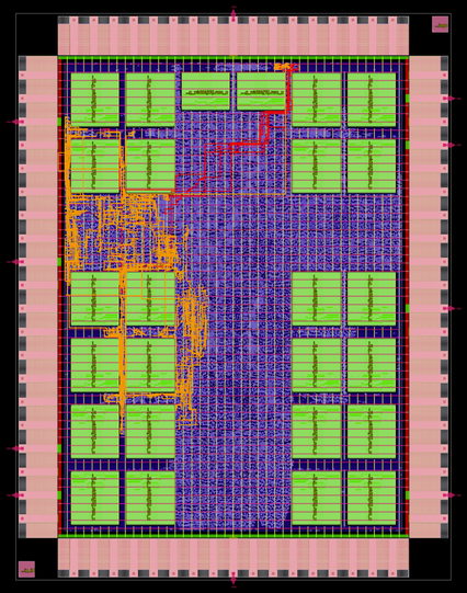
Day 6: brought up software execution on both cores from internal RAM. Wrote audio output pipeline for the APU. The orange/red here is the clock tree insertion for the audio clock domain; I might have over-egged it with the filter taps. Also APU has full RV32I register file now.
One thing I noticed from looking at how the Hazard3 register file is mapped with clock gating inference enabled: register 0 (x0) is present and correct in the netlist even though its output is always squashed in the next pipestage. Oops.
I've always kept the actual regfile code completely uniform to preserve BRAM compatibility, but maybe it's time to make that a bit uglier (in a generate block). I'm also interested in latch-based register files but the constraints could be interesting.
The CG inference looks correct, and I am getting the smallest flop type with one CG per 32-bit register, so nothing to complain about there.
Can I just say how nice it is to open the netlist for an entire chip without bringing my text editor to its knees?
I heard you liked YAML so I put YAML in your Python in your YAML
Not sure how I made it this far without making one of these tools:
This is the crt0 for my bootrom. Think this has a good amount of silly stuff going on for 30 bytes of code.
Also I'm not going to write ELF patching to fix it but it still annoys me that GCC stacks registers on entry to a `noreturn` function. What are you planning to do with those bro?
Ok, I'll be honest. The tools are kind of rough.
Looking at a latch-based register file for Hazard3 with ICGs to generate the latch enables. Was looking good up until CTS inserted a clock buffer with only its output connected in between one of the ICGs and exactly one of the latches. I don't think that's going to pass LEC...
I don't need formal equivalence checking to see that one of these things is not like the others 🥲
New latch register files. Still a lot of cells and routing, but yeah, there's 1 kbit 2R1W in each of these 😅 timing is a little better
Also I realised I was being dumb with the FIR filter implementation so that should come down in area quite a bit.
For a density comparison on the register files, each of the square RAM blocks is 512 x 8, so 4 kbit single-ported.
Tonight on man vs tool
At this point I have the entire timing table from an async SRAM datasheet pasted into TCL comments
cocotb's promises of effortless software cosimulation are slightly undermined by the 100% overhead associated with toggling a clock from cocotb instead of from Verilog
Left it quite late in the project, but I brought up some simulations for the CPU executing from external SRAM. Very minor detail of the WEn appearing on the wrong clock, but chooches happily now that's fixed
I was bringing up these sims in between STA runs (ongoing hostage negotiation with OpenSTA about the SRAM timing) and managed to find a bug in iverilog at the same time: it seems to have infinite compile time for the async SRAM model I successfully used on RISCBoy. Having bad luck with tools today it seems.
Sticking a UART on a GPIO alt function because why not. It wouldn't be a 2000s ish console if it didn't have infrared, so I can have a small extra feature, as a treat:
It's pretty cool that I can file a GitHub issue about DRCs on standard cells. Feels like progress
https://github.com/wafer-space/gf180mcu-project-template/issues/34
Have 70 ps hold violations. Add 80 ps of hold margin. Result: still have hold violations, and setup is 2 ns worse.
This is why we don't try to fix CTS issues by resizing buffers on the datapath
Contemplating some manual buffer ECOs to balance this clock tree, once my synth netlist is locked in. Not to say "I could do this better by hand" but I could do this better by hand
Big news: there is a Bigger Clock Buffer.
I finished the design (and probably all the verification) of the streaming SPI read peripheral for the APU. It's fairly simple, the only neat trick is the CPU can reach in and pause the stream so it releases the SPI GPIOs. The CPU can squeeze in a quick access to something else, like the shift register for the buttons, then un-pause the stream and it picks up where it left off.
I don't have a system DMA so having this integrated into the APU is a neat way to support streaming audio samples (ADPCM etc) from flash.
The last new thing to design is the clock generators. This is probably just going to be a dumb divide by 1 or 2 circuit, separately controllable for LCD clock, system clock and audio clock.
If like me you were worried about whether the GF180MCU mux2 had a static hazard when switching between two equal inputs, I have good news: it does not
This is all the clock configuration you get. The LCD SPI SCK is always sourced directly from the clock pad. Main target configuration is LCD clock 36 MHz, system and audio clocks at 24 MHz.
It's structured as multiple fixed dividers with a glitchless mux, because synchronising controls into a programmable divider is kinda subtle and I'm not confident in constraining it correctly.
Not sure how usable the 2/3rds division is going to end up being since I kind of need 50/50 duty cycle to get correct timing on the SRAM WEn pin 🤔 but it's harmless to chuck it in. Being able to patch the debug clock in as a secondary clock source lets me experiment with other ratios.
Processor switching its own clock!
Another day, another show-stopping OpenSTA + OpenROAD CTS bug. Actually it's hard to tell whether it's a bug due to the sparsity of the docs, but I'm pretty sure OpenSTA is propagating an upstream clock through a buffer that is already defined as the root of a different primary clock (output of a clock generator that doesn't need to be balanced against anything else in the design). As for CTS, it seems to be trying to balance everything against everything and predictably failing. I thought I was going for a simple design here that would be easy to constrain.
Escalating options:
1. Just backhand the tools like below
2. Define functional clocks as generated clocks with one source and a fixed divider (feels wrong because it implies a phase relationship and these are async clocks, then again not convinced CTS sees anything in the .sdc anyway)
3. (tactical nuclear) Create a new liberty cell which is a copy of the clock buffer but has the buffer logic function removed
4. (strategic nuclear) Harden a macro for my clock generator so I can abstract the timing
I don't know this for sure but I think most chips taped out with these tools have had, like, one clock coming in from a pad
API listing: -source is a pin.
Examples: -source is a clock.
Experimentally: passing a clock raises an error saying it's not a pin
@wren6991 if it’s any consolation, commercial tool documentation isn’t really better. In their example, it works because both the clock and the pin are named the same. Not a good example.