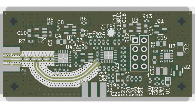
A week ago I posted here a PCB design I've been working on with an ADF4158 and HMC391 for the LO of an FMCW 10 GHz radar. Thanks to all who reviewed this and sent suggestions. I have now switched to a 4-layer FR4 stackup, added M2 mounting holes and done other tweaks. Probably I will send the board to the fab sometime this week. Until then, there is still time to give feedback: https://github.com/daniestevez/ADF4158_PCB
GitHub - daniestevez/ADF4158_PCB: ADF4158 + HMC391 PCB for 10 GHz FMCW radar LO

ADF4158 + HMC391 PCB for 10 GHz FMCW radar LO. Contribute to daniestevez/ADF4158_PCB development by creating an account on GitHub.

GitHub

@destevez This version looks much better to me.

The main thing that still stands out to me is the use of thermal reliefs on the copper pours. In general these are usually best avoided for GHz work. But they do make things easier to hand solder. Again, I don't think it's anything that will stop this board from working, just general advice.

@martling There are 10 vias in each of the SMA ground pads, and groundplane below it. These cannot be seen in the 3D render because it renders the solder paste on top of the vias (probably there is a way to tweak this, but I haven't messed around with the render settings).