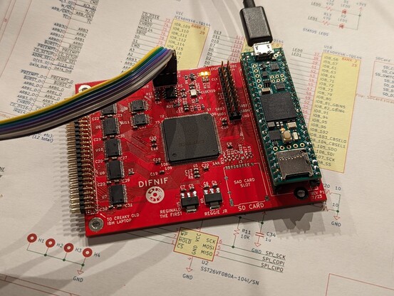
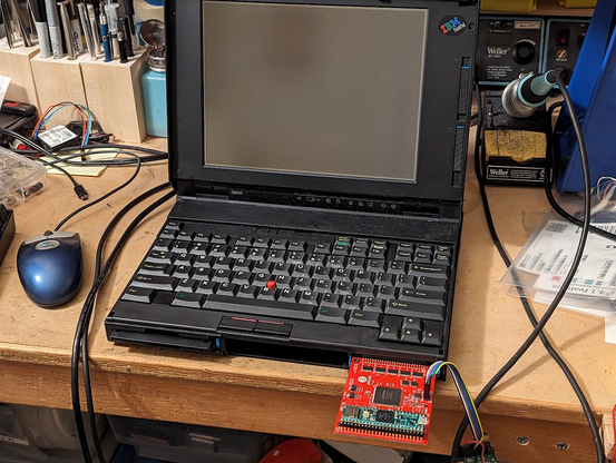
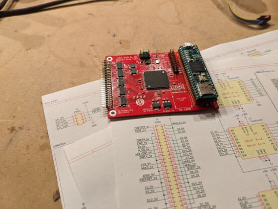
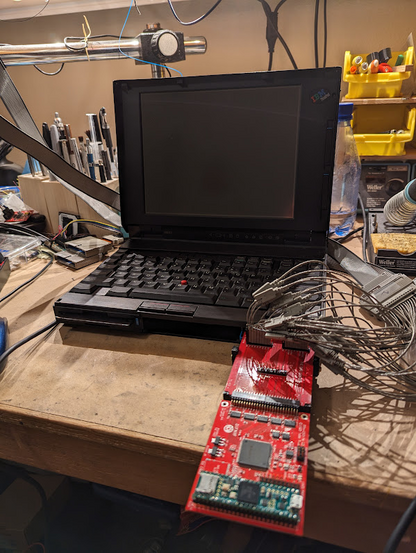
I'm working on a new FPGA project. this one is rather complex.
I'm at the "blink an LED" stage of bringing it up.
wrote some temporary verilog to validate the bus interface using a single 16-bit register. here goes nothing
oops. logic analyzer time. guess i should have expected it.
ok so i unplugged the board and powered up the computer -- and the error stays. looks like i broke something. 😩
gotta take this step by step. I should have checked this at the start but first I will force the FPGA into the unprogrammed state (-CRESET low) then check each pin to make sure it's in a valid state.
ok when *not* in reset, the FPGA is pulling the DMA line BURST_L low constantly. this is bad, and explains the 00011320 error i saw earlier.
seems that i typo'd the wiring between the top level verilog module and the module that handles the micro channel bus. it's a floating connection and it seems to mostly just sit at a logic 0.
the other problem (01290200) is more concerning and will need a logic analyzer.
yes, i made a dedicated interposer/extender board just to help with the logic analyzer connections. it's called the Fing Longer (a reference to Futurama).
hmm, so during a read operation, the data is never driven onto the bus (the output stays pulled up to FFFF). looks like the MADE24 line is staying low? that's weird. let me try making the logic ignore it.
oh! now the card is putting data onto the bus! the "test1" channel is the data direction for the 74lvc4245 buffers showing that they are transferring data from the card to the host PC.
wow, it actually works, i'm able to write a value to the simple register and read it back. this is a HUGE step forward.

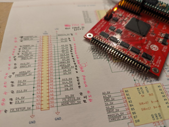
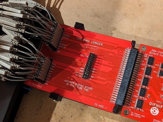
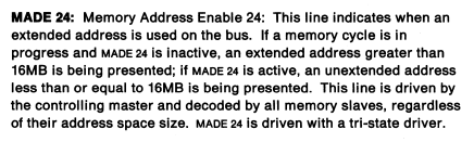
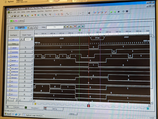
i'll need to figure out what is up with the MADE24 line. could be that the pin doesn't actually do that. the HDD pinout is one that i reverse engineered a while back, so it might be a mistake.

this could also explain the damage to the PC, perhaps the card tried to write to the data bus when it was not supposed to and damaged the output drivers of some other chip.

huh, the "MADE24" line is controlled by bit 7 of register 96. I wonder what that is.
lol, this is the active high CHRESET! i was wondering why that line seemed to be missing.
moving on to the Teensy interface. i had to choose the IO pins carefully so i can make a 16-bit parallel IO port.

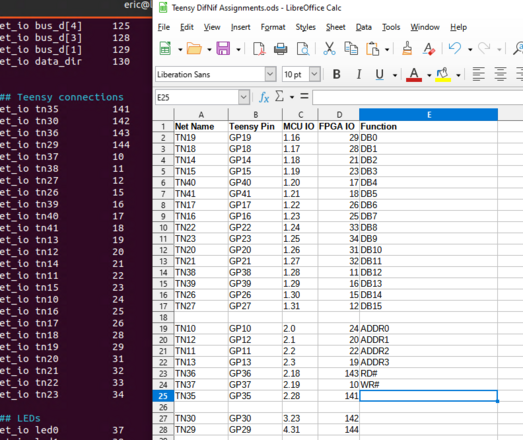
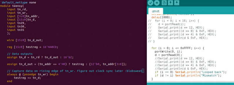
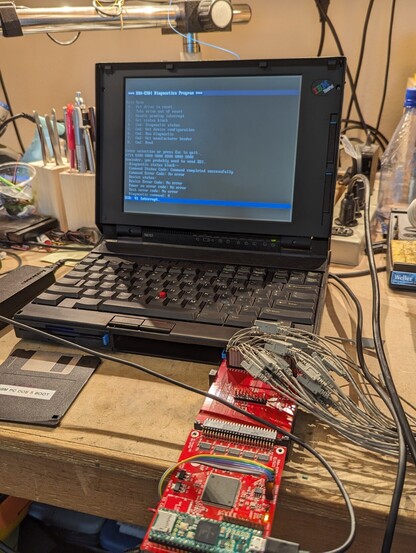
got the Teensy interface up and running. i'm using direct IO port access on the Teensy 4.1. take a look at core_pins.h in the Teensy header files. basically you can read from GPIOx_PSR and write to GPIOx_DR.

i also had to add a short delay to create some setup time for the FPGA--the Teensy 4.1 is a hair too fast lol

bidirectional registers now work! i can write a command from the PC to the Teensy, and i can write a response from the Teensy and read it from the PC. there are also status flags showing when new data is available. it may not seem like much, but this is huge progress.
excellent progress today. I've been able to implement the "Get Diagnostic Status" command. it transfers the command block and handles the returning status block as well as the flags and interrupts. best of all, it works on real hardware using my diagnostic program!

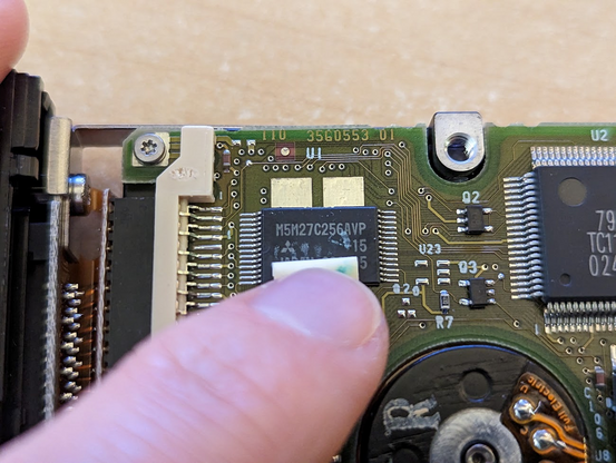
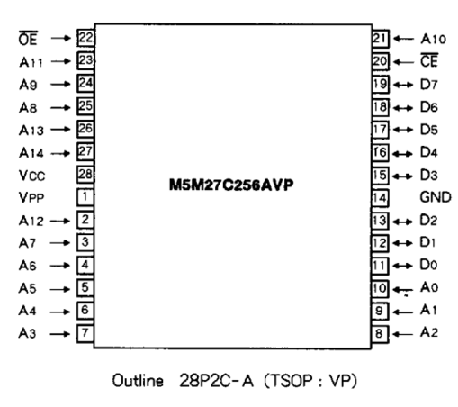
OK why does pin 1 start halfway down the edge of this chip???

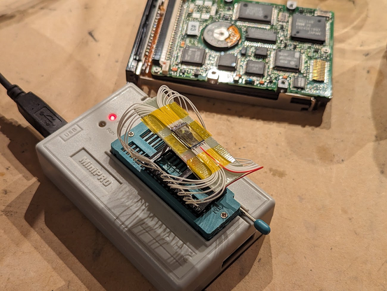
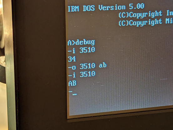
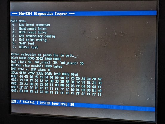
my best guess is that the die is rotated to a 45 degree angle. anyway i want to dump the contents so i can analyze the drive firmware.

no 28-pin TSOP socket, oh well
now i'm knee deep in Ghidra listings. this code probably runs the entire hard drive, not just the host interface.
this sort of reverse engineering is very much like solving a challenging puzzle. you push and push until you can deduce something based on what you already know, then you pivot, taking that new knowledge and pushing on that until you learn even more.

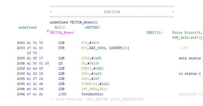
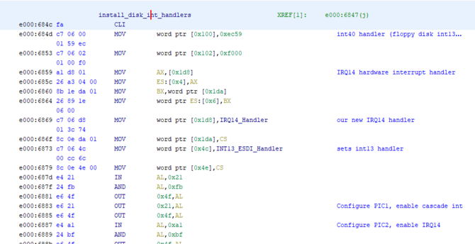
so last night I identified the power on self test routines by inspection. it's not too hard to identify a checksum routine or a memory test routine. this helped me fill in the memory map.

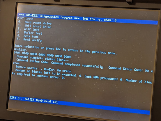
also, the POR test function stores the results at a particular memory location, and the codes match up with the POR error codes in the DBA-ESDI spec! the next step is to search the whole ROM for any instructions that read this memory location--this should identify the functions that generate the status block.

drive firmware is turning into a bit of a slog so i switched over to the IBM BIOS. having a spec is nice, but the code will cover a bunch of corner cases.
managed to reverse engineer enough that I was able to read the defect map out of one of the original hard drives. sounds easy but the process uses DMA.

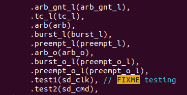
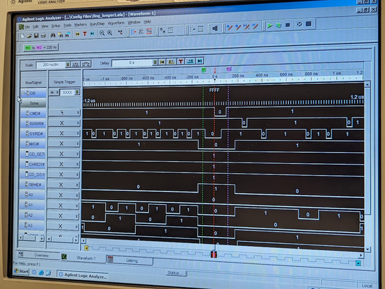
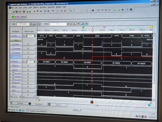
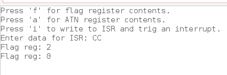
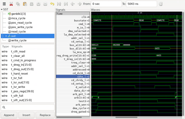
working through a nasty timing hazard with the mailbox flags on the command port. sometimes you write data and the "data available" flag never gets set.

so now i am digging through the logic that yosys generated to see if it even makes sense.

having good test programs is important. here's the status interface register dropping values. the Teensy program is just writing an incrementing number, and the diagnostics program is checking for gaps.

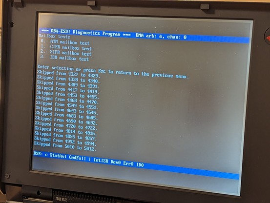
got that all sorted out. it was a synchronization issue with the flags between the two interfaces.

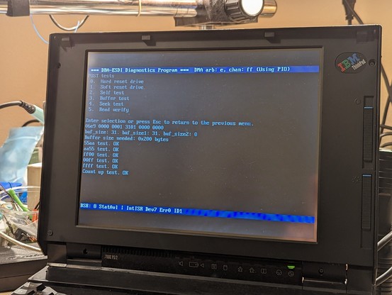
this is the "seek" command successfully completing! this is a *major* step since it requires 4 working mailboxes and interrupts.

another important step today--i got the data port and data port mailbox flags working. it can also detect 8-bit vs 16-bit transfers. getting very close to working PIO transfers.
nice! I managed to get PIO data transfers working well enough for the buffer test routine to pass.
ok this is fantastic--I've managed to transfer my first actual sector! it's just using PIO and the data is not from a real filesystem, but this is another big step forward!

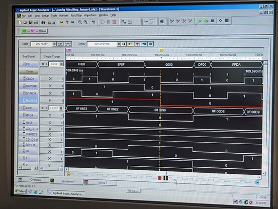
DMA on Micro Channel is really hard. i'm running a bunch of simulations first, making adjustments to the logic as needed.

so many moving parts.

wow, got four bytes to transfer successfully over DMA! not sure why it got stuck after that.

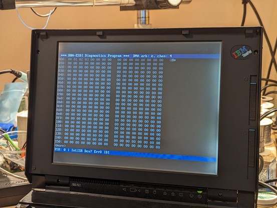
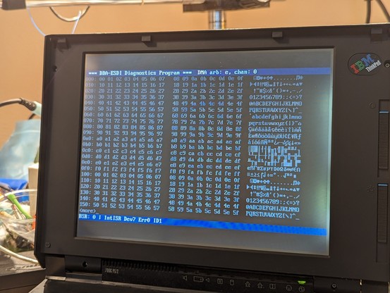
just ran the same test again and it transferred the whole sector over DMA!!

so at least read transfers are working partially. writes just hang the machine after transferring half a sector. it's probably time for the logic analyzer.

@tubetime I wonder if IBM expected you to use a special chip that did a lot of that for you.
@tubetime Almost makes you want to lovingly caress it's slightly sticky chemically degraded surface. 😉
@tubetime mailboxes means what exactly here?
@1000millimeter these are registers accessible from two different CPUs, so they have to be synchronized using mailbox flags. basically a bit that gets set automatically when a register is accessed by one CPU that can be seen by the other CPU.
@tubetime
If a computer can't count straight, it's not a good sign.
@tubetime I've lost count of the things I've done that "sounds easy but the process uses DMA."
@tubetime I miss simple DMA controllers. Sure, the new ones are all-singing, all-dancing, platinum-plated, but when you just need something simple, they're a huge pain.
@brouhaha most recent SoC i used had a DDR3 controller with around 800 configuration and status registers. 800!
@tubetime And for all that modern DMA controllers are super-fancy, AFAICT none of them support address decrement on either source or destination. Admittedly that's a lot less common than increment, but I've had occasions where it would have been very useful. In the 1970s and 1980s, some DMA controllers could do it.
@brouhaha @tubetime ...and then you have DMA issue that affects all the peripherals. Just recently I had this pain with nRF52832 SoC - https://github.com/embassy-rs/embassy/issues/460
Mitigate nrf52832 dma errata · Issue #460 · embassy-rs/embassy

https://infocenter.nordicsemi.com/pdf/nRF52_PAN_109_add_v1.1.pdf

GitHub
@plaes @tubetime I encountered trouble with the nRF52832 DMA in 2019. May or may not have been the same issue. I don't think the errata for my issue had been published yet; I had to file a support ticket.
@tubetime Out of curiosity, does the newer IBM BIOS have any similarity to the original IBM PC AT BIOS that they published in the AT Tech Reference from March 1984? Wondering if they ever did a full rewrite at some point. http://bitsavers.trailing-edge.com/pdf/ibm/pc/at/1502494_PC_AT_Technical_Reference_Mar84.pdf

@tubetime

Meme image: good news bad news.jpg
Top text: successfully locating the reset vector in a piece of mystery code
Bottom text: realizing that the code starts doing weird stuff when you’re only 5 instructions into the reset vector

I have mainly reverse engineered things with user interfaces, so there’s always strings I can work backwards from. Doing something like a hard drive controller is playing the game on extra hard mode.

@tubetime you don’t drink enough coffee. ;-)
@smitty @tubetime 100% I follow @tubetime cause he’s crazy x10. Feels like I’m back in time watching a self study senior electrical engineering lab - except it seems he always gets it to work.
@tubetime Beautiful organized chaos ✨
@tubetime you gotta do what you gotta do
@tubetime I once bought the wrong form factor AtMega 8...
@tubetime What is that yellow tape? See that sometimes on Electronics but don't know where to buy or whats special about it.
@1000millimeter kapton tape, sometimes called polyimide tape.
@tubetime I’ve always wondered about that. I think your intuition is accurate since that would allow a smaller package size from less area outside the die needed to route to the external pads.
@tubetime It's two! (click) two! (click) two chips in one!
@tubetime It's at least so common that the Altium footprint generator has an option for it, although I have never seen it in the wild on any chip sp far.
@tubetime A lot of early quad SMD packages numbered starting in the middle of the "top" side, and that was purely a (dumb) thing done by package vendors, and dice were always still mounted orthogonally. (or perhaps _almost_ always)

@brouhaha @tubetime I know PLCC still is numbered this way. Weird to see it on a chip with legs on only two sides.

Edit: just noticed its otherwise a standard Eprom pinout just with the odd pin one location. How weird.

@ChartreuseK @tubetime Oh, I somehow overlooked that it was dual rather than quad. Definitely an oddball.
Great progress! But help out simpleton me, I've lost track of what you are doing. Is this still part of reverse engineering things to get a SnarkBarker to work on the expansion port?? Or an entirely different project?
@darryl_ramm it is a solid state replacement HDD that works with the weird IBM DBA-ESDI protocol (similar in concept to IDE)
@tubetime Cool, I would love to get a 701 butterfly. Had one for years at work.
@tubetime 16-bit parallel sounds like HPIB.
@fozztexx it's because DBA-ESDI is also inherently 16-bit. weird, but i must say that 256-word sectors is actually kinda satisfying.