Small Microcontroller Displays

I found myself wanting several small displays connected to a microcontroller, so was doing a bit of a trade-off between various options, and was starting to lose track, so this post collects some of those thoughts together.

It is not meant to be a comprehensive discussion of choosing small displays for projects, but more of a reflection on the displays I already have kicking around in my parts boxes!

Most displays tend to be categorised by the driver chip they use. And then by the bus type used for their connection. So that is how I’ve grouped them here.

A really good reference for many of the displays shown here is: https://www.lcdwiki.com/Main_Page

I2C SSD1306 OLED

This is usually my “go to” set of small displays. They are generally well supported and pretty easy to use.

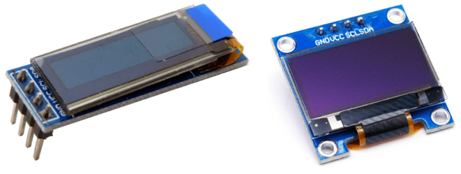
I generally have two variants to choose from:

On the left is the 0.91″ 128×32 OLED SSD1306 and on the right is the 0.96″ 128×54 OLED SSD1306. Common properties of both displays:

  • Monochrome – white or blue.
  • I2C interface.
  • Usually 5V powered, but some include level shifters to allow 3V3 logic.
  • Usually includes I2C pull-ups. Might be to VCC level so be wary if using a 3V3 MCU but powering from 5V – always check the voltage level prior to connecting.
  • 128×32 usually a fixed I2C address (0x3C). 128×64 usually allows selection between 0x3C and 0x3D.
  • There are variants with VCC and GND swapped, and other variants with SDA and SCL swapped.

Software support:

Typical Connections:

  • VCC/GND (see note below re VCC vs logic levels).
  • SCL/SDA – I2C pins on the MCU.

Known “gotchas”:

  • Requires a chunk of memory allocated on start-up on Arduino, which can fail if there isn’t enough dynamic memory left and make a sketch hang.
  • Can’t be written to from an interrupt routine (e.g. a timer).
  • Low-level I2C Wire library on Arduino is blocking.
  • Can sometimes be a little slow compared to alternatives.
  • Limited I2C address options, so multiple display use is limited (and also increase the memory issues).
  • As already mentioned, any I2C pull-ups may be pulled up to the VCC level or might be level shifted, so it is always worth checking if planning to use with a 3V3 microcontroller.

Summary:

  • Cheap, pretty easy to use, and fairly universal if you want a single, small, monochrome display for simple outputs.

Other I2C Variants

There are some variants of the SSD1306 that sometimes pops up too for slightly larger displays:

  • SSD1315 – apparently can simply be treated as a SSD1306 and mostly it works ok.
  • SH1106 – very similar niche to SSD1306 but requires it owns driver support.

SPI ST7735/89/96 TFT

Whereas the SSD1306 I2C is pretty ubiquitous for monochrome displays, I’ve tended to find that SPI ST77xx displays fill a similar niche for small, full colour, non-touch, TFT displays. And there are loads of variations on the theme when it comes to these displays.

The 7735 supports lower resolution, smaller displays, typically up to 170×320, with the 7789 for those of 240×240 or 240×320 and similar. There is also a ST7796 which I believe uses the same driver libraries for a higher 320×480 display.
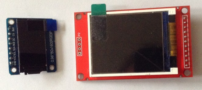
Two 7735 Displays:

These two ST7735 displays that I have are labelled:

  • TFT 0.96″ 80×160 SPI ST7735
  • TFT 1.8″ 128×160 SPI ST7735

These ST7789 display I have is labelled:

  • TFT 1.3″ 240×240 SPI ST7789

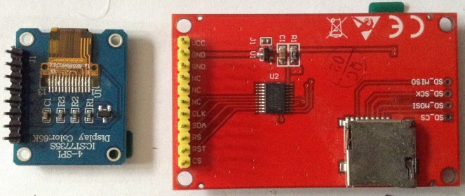
I also have a display that was bought as a ST7789 labelled “TFT 2.8″ 240×320 SPI” which comes with a touch screen, but I can’t get this to work.

Common properties:

  • SPI interface: data (SDA/MOSI/COPI), clock (SCK/SCLK), chip select (CS), data/command (SR/DC), possibly a reset.
  • Typically 65536 colours, usually encoded as 5-6-5 bit RGB patterns.
  • Have to check for 3V3 or 5V operation depending on the datasheet of the driver chip and design of the module.

Software support:

Typical Connections:

  • VCC/GND
  • CLK/SDA – SPI Clock and Data (Data OUT from MCU – i.e. MOSI/COPI)
  • RES – Reset
  • DC, RS – Data/Command Register Select
  • CS – Chip Select

Known Gotchas:

  • Working out if RS means reset of the data/command pin; and not mixing up SCL/SDA with I2C!
  • Some might include a backlight control pin too for dimming or turning it off. With this not connected the display was a maximum brightness.
  • I’ve also seen talk that many of these modules themselves run at 3V3, so whilst they may include a regulator for 5V to 3V3 for power, they don’t always include level shifting for the signal pins. It seems unclear (to me at least at the moment) if it is ok to use these with a 5V microcontroller (although I have done…).
  • Some of these displays are “inverted” colour wise. The use 16-bit 5-6-5 format colours, but some are RGB, some are BGR and there might be other variants too.
  • Sometimes the initialiser for the library requires a SPI_MODE setting. My ST7789 240×240 required the Adafruit ST7789 initialisation as follows:
#include <Adafruit_GFX.h>
#include <Adafruit_ST7789.h>
#include <SPI.h>

#define TFT_CS 10 // (not used)
#define TFT_RST 9
#define TFT_DC 8

Adafruit_ST7789 tft = Adafruit_ST7789(TFT_CS, TFT_DC, TFT_RST);

void setup() {
tft.init(240, 240, SPI_MODE2);
}

Note, unlike the monochrome displays, these have their own pixel framebuffer so memory use is much more efficient, even when used as a full colour display.

Summary:

  • Cheap, pretty easy to use once the voltage levels and the pin labelling are worked out. Well supported by a number of libraries; but does require more pins for 4-wire SPI. Might need some messing around to get the right colour definitions. Otherwise a good choice if you just want a cheap, colour display with no touch.
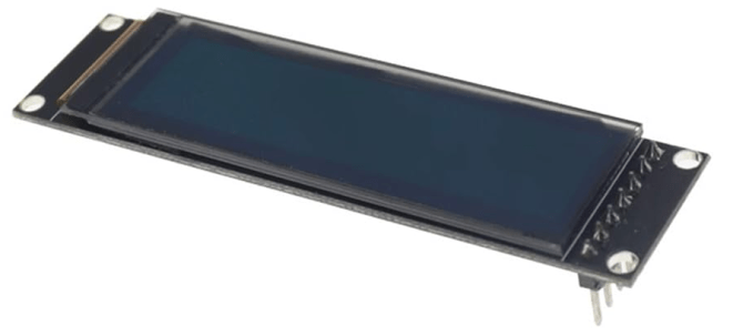
OLED SH1122 SPI

There are actually both I2C and SPI versions of SH1122 displays, but I’m considering the SPI version here. The display I have is a 256×64, monochrome OLED display.

Software Support:

Example:

U8G2_SH1122_256X64_1_4W_HW_SPI u8g2(U8G2_R0, /* cs=*/ 10, /* dc=*/ 9, /* reset=*/ 8);

Typical Connections:

  • VCC/GND – mine states it can support either 3V or 5V power
  • CLK/SDA – SPI Clock and Data (Data OUT from MCU – i.e. MOSI/COPI)
  • RES – Reset
  • DC, RS – Data/Command Register Select
  • CS – Chip Select

The _F_ constructor requires a full frame-buffer so is unlikely to work on resource constrained devices (e.g. the Arduino Uno/Nano). The _1_ constructor provides a pageable interface which allows for the updating of the display in pages, which takes longer but allows it to be used with more devices.

There are also software SPI versions that allow the use of any GPIO pins.

Summary:

  • A pretty neat board if these physical dimensions match what is required.
  • There are a whole pile of example sketches in the U8G2/page_buffer directory.

ILI9341/9488 TFT

Cheap larger displays are often driven by one of the ILI9341 or ILI9488 chips. The former supports 240×320 in full (16-bit) colour whereas the 9488 tends to support larger displays of up to 320×480 in full (24-bit) colour. Both support either a parallel (at least 8, 9, 16-bit) or serial (3 or 4 wire SPI) bus interface.

I don’t have a lot of detailed information for this post yet, but instead will refer to:

The ILI9341 is well supported by the Adafruit graphic libraries, but the ILI9488 is likely to require something else, as described in the above post.

These displays are often used with touch support and will often expect to run at 3V3 logic levels.
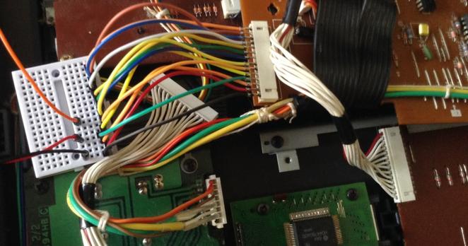
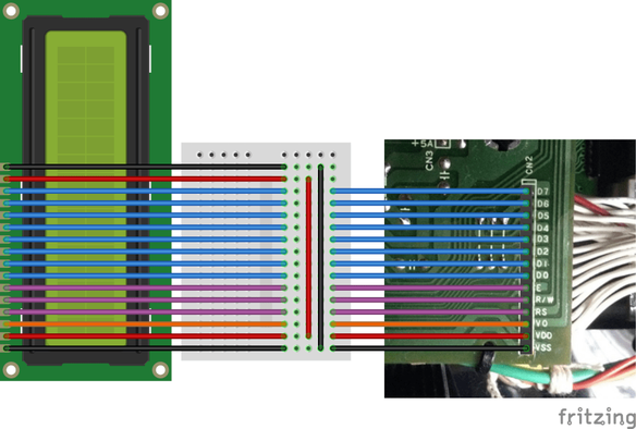
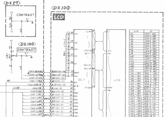
LCD 1602 HD44780

This is another very common monochrome, but text only, display. They have a 4 or 8-bit parallel interface, but it is also quite common to use the with an I2C “backpack” based on the PCF8574 I2C IO expander. Boards can be cheaply bought with or without a backpack, and the backpacks are available separately too for retro fitting to displays without them.

They are often called “1602” displays as they are two rows of 16 characters. By using custom blocks it is possible to have some simple graphics. There are LCD2004 modules too with four rows of 20 characters.

They often come with a choice of backlight colours. White or red are particularly striking! There are some variants that come with an additional I2C controller chip built in to control the backlight and some even come with a full RGB backlight capability.

Typical Connections:

  • VCC/GND
  • Data – either 4 or 8 bit modes support
  • E, RW, RS – enable, read/write, register select.
  • Backlight V+/GND – level is often fixed using a resistor.

There are core Arduino libraries to support the most basic versions of these displays:

  • LiquidCrystal
  • LiquidCrystal_I2C

Typical Gotchas:

  • The I2C backpacks often include pull-ups to VCC, yet many of these displays require 5V even if used with a 3V3 microcontroller. One option is to remove the pull-ups and add external pull-ups to 3V3.
  • If there are only blocks on the display then the communications isn’t working properly – check SDA/SCL or the control lines.
  • If there is nothing on the display or the text is obscured by blocks behind it, then the contrast is either too low or too high. I2C backpacks have a potentiometer to adjust the contrast.
  • More complex versions require an additional I2C setup phase, e.g. to turn on the backlight, which isn’t supported by the standard libraries.

Summary:

  • Very useful if a large, high/adjustable contrast, text-only display is required.

Others

So I don’t forget when considering the above, I also have:

I’ll add to the list for my own reference as I remember other odds and ends.

Kevin

#hd44780 #ili9341 #ili9488 #include #lcd1602 #oled #ssd1306 #st7735 #st7789 #tft

Diagnosing and attempting to fix a Yamaha DX100 – Part 4

I decided to have one more look at the data pins, largely inspired by this oscilloscope trace from part 3. I figured if the address and select pins were working (yellow, cyan and purple) what could I do to try to work out what is driving the data pins (darker blue) wobbly…

And no, after all this time, it still isn’t working…

Warning! I am not an electronics person. I strongly recommend that you don’t base your own attempts at fixing a beloved vintage synth on anything I’ve said here. I was given this synth rather than it being sent it to a recycling centre so this is a low-risk learning activity for me. I am not responsible for any damage to expensive or irreplaceable electronic musical instruments! There are plenty of places to take something for a proper repair 🙂

If you are new to microcontrollers and electronics, see the Getting Started pages.

Pulling D0 to LOW

My first thought was to see if I could use a weak pull-down resistor on one of the data pins (I was using D0) to see if that stabilises the signal and then see what the data trace looks like as I move around monitoring the various chip select/chip enable lines.

So with the replacement LCD attached from last time, I hooked up the following:

  • Oscilloscope GND to GND.
  • 10K between GND and D0.
  • Oscilloscope tracing LCD E pin.
  • Oscilloscope tracing D0.

Unfortunately whilst it did stabilise the data signal a little, it still wasn’t really clear what might be causes the issue.

It did give one other clue though. When testing the RAM chips, I could see the data signal was actually quite clear when the RAM /CE was active (LOW).

So I abandoned that and tried something else…

Closer look at the Data Lines

So given the observation about the RAM chips, I decided to take a proper look at the data lines (well D0) when the various chip enable/chip select signals are active.

Handily, as the PCB is a single sided PCB with bridging wires, it was relatively straight forward to find wire links for both GND and D0, so I used these for the oscilloscope GND and blue trace (for D0).

The two probe GNDs are pushed under the link on the bottom left and D0 is the first of those block of links after the first three top right. This leaves a free-floating probe wire for me to use to prod the various select lines and see what D0 is doing at the time.

So, starting with the two RAM chips, /CE is on pin 20 and the trace I obtained looks like this:

On the face of thigs that still looks pretty chaotic, but actually the data signal (blue) is stable for the duration of the /CE signal being low, so that is probably actually ok.

A similar pattern was observed for the other RAM chip and the Yamaha OPP’s /CS signal.

The ADC is a little more complicated as can be seen in the extract from the schematic:

There are sort of three relevant pins here: 6 (START), 9 (OE) and 22 (ALE). IC17 is acting as an inverter so that when ADDAT and RD are both LOW OE is HIGH.

/ADCH and /ADDAT come from the address decoding logic:

But the upshot of all this is that when any of these signals is active, D0 looks pretty similar to the RAM trace.

So at this point, I’m feeling a lot more confident that the two RAM chips, ADC and OPP are probably not at fault.

The ROM is next on the hit list. Now again, looking at the schematic we can see that the ROM is enabled when A15 is HIGH (address $8000-$FFFF) and this happens thanks to another gate in IC17:

So the ROM is active when /CE is LOW, meaning A15 is HIGH. But when traced on the scope, D0 is all over the place (blue), especially when /CE is low (yellow).

It is curious to see that the ROM seems active for a lot longer than any of the other accesses I’ve examined. But I guess if the CPU is running from ROM it will be continually reading instructions whilst shuffling data between the other peripherals.

But regardless, I’m now very suspicious of this ROM.

The inverter is IC17 and also drives LCD E, which also doesn’t seem to work very well.

So even though I tried a new ROM and nothing seemed to change, I replaced the ROM again and actually took a proper look at the signals on the bus.

That seems to speak for itself. Yes, /CE is still LOW for larger periods of time, but those data signals are massively improved.

Spoilers: it turns out this wasn’t what I thought was happening, but I’ll get back to that in a mo…

So this is now what the LCD E triggered trace looks like.

That looks like a massive improvement! So why isn’t this working now then?

Not so fast… I messed up the ROM

So now I have half the display showing blocks, a flashing power LED and still no other signs of life.

A flashing LED apparently indicates that the backup battery is low. This in and of itself is probably progress as the LED is connected to an IO pin of the CPU, so this seems to indicate the CPU is actually running code as it is making the LED flash. So why isn’t it booting?

Measuring the voltage from the test pins, it is reading 2.7V, when I think it is meant to be 3V.

I’ve not managed to get a replacement display running by plugging wires into the socket instead of the original LCD. But scanning all the data lines of the display when it is enabled, seems to show they are all working ok.

So the question is now:

  • Has the CPU got stuck in a loop with the flashing LED? It’s certainly possible.
  • Or is the display not functioning properly?

Well it turns out there is another condition where the LED flashes.

As I was poking around I noticed there were some fairly regular repeated patterns on the address bus, and it seemed like the RAM wasn’t being accessed anymore.

It turns out another condition where the LED flashes is if there is no code in the ROM…

Yes, I’d put in a blank ROM by mistake. Sigh.

Unfortunately when I program the ROM (and verify it) and plug that back in, the black squares on the display have now gone, but the data bus is messed up again.

I guess that probably means it isn’t the ROM that is at fault.

But that probably points to something that isn’t enabled properly until some code is running on the CPU from the ROM.

Mind you, I don’t know what allowed me to get the LCD trace if there was no code in the ROM… but I guess the CPU could have been doing anything at that point.

So About that ROM

At this point I wondered what it all looks like if I unplug the display. And yes, sure enough, the signal is a lot cleaner again.

So, does unplugging the display fix things because the display is causing the issue? Or does not having a display change what code is running so the problematic peripheral or mode is missed out (like it was when the ROM didn’t even have code)? It’s a little hard to say.

At this point I thought I may as well go back to the original ROM. After all it is a lot nicer to have one stamped Yamaha than one stamped 29C256. But then something else interesting happened. Here are two traces still without the LCD connected:

The one on the left is the replacement, reprogrammed 29C256 flash EEPROM and the one on the right is the original Yamaha mask ROM. In both cases the ROM is enabled when the yellow trace is LOW and the blue trace is D0. As we can see, there is still something not right about the original ROM…

LCD Enable and Data

Assuming that the ROM is now fixed, there is something odd about the LCD. I’m not convinced my Heath-Robinson mashup of a breadboard and 1602 LCD is giving me any results I can rely on, but I did one last experiment.

As I wasn’t sure if removing the LCD prevented the actual issue or just stopped the code from enabling a different problematic peripheral, I wondered what would happen if an LCD was connected, but I just removed its ability to drive D0 whilst I was monitoring it.

Here is the result. On the left, with D0 connected to the LCD, on the right with D0 unconnected.

It does seem to be better when D0 can’t be driven from the LCD (LCD enable, and other data lines are all functioning normally). There is a single access on power up, then another one maybe a few 100mS later, and then a burst of activity, and then nothing at all.

I wondered if maybe the logic controlling the E (enable) line for the LCD might not be working properly, so I went back to the original LCD and took at a look at LCDE.

Homing in on IC17, I should be able to see a LOW signal on pins 5 and 6 generating the HIGH E (enable) signal for the LCD, and yes, that appears to be working fine as far as I can see. This is a sample of the “busy” set of accesses just prior to everything going silent.

So going back to looking at the data lines (D0) whilst this is going on…

Sp there doesn’t seem to be an issue with the data lines whilst the LCD is being poked (left). But when the accesses to the LCD appear to stop (right), then the data line seems to be all over the place once again – it gets worse after this initial activity.

But there does seem to be some kind of pattern here, which implies to me that everything is stuck in a loop somehow. Here is the zoomed-out version of the last trace, showing the last of the LCD Enable lines and the following patterns in data (zoomed back in on the second trace).

Conclusions for now…

So where does this leave me? To be honest I’m not sure. Maybe back where I started.

It would appear that with the display out of the loop there was something screwy about the original Yamaha ROM. But I’m not convinced that the display isn’t causing issues too.

I’d like to take the display PCB apart and check connections and clean it, but it has one of those flexible connectors between the controller PCB and the LCD display, so I’m not sure I want to mess with that right now.

If I can find a robust way of plugging in an alternative display I might give that another go.

Either that, or I might return to the power circuit as that 5V line does seem pretty noisy to me.

When I decide on next steps, I’ll come back and add to this post again.

Kevin

#dx100 #eeprom #lcd1602

Diagnosing and attempting to fix a Yamaha DX100 – Part 3

At the end of part 1, I’ve established that the basics all seem ok (PCB, interconnections, power) and that basic digital logic stuff is happening.

In part 2 I checked the ROM, reflowed a number of the solder joints, and started to look at the connectors between the main PCB and the LCD, but still with no luck.

Now I’m finally getting around to looking properly at those data signals to see what my next steps might be.

Oh and nope, still not fixed. Sorry.

Warning! I am not an electronics person. I strongly recommend that you don’t base your own attempts at fixing a beloved vintage synth on anything I’ve said here. I was given this synth rather than it being sent it to a recycling centre so this is a low-risk learning activity for me. I am not responsible for any damage to expensive or irreplaceable electronic musical instruments! There are plenty of places to take something for a proper repair 🙂

If you are new to microcontrollers and electronics, see the Getting Started pages.

Replacing the LCD – Continued

In part 2 I thought that it would be worth seeing if I could replace the LCD with an alternative, seeing as it appeared to be just a common HD44780 based display, but the connector used was giving me trouble.

In the end I just took the plastic shrouds off some Dupont style jumper wires and poked them directly into the connector on the PCB.

This finally gives me a way into some of the control signals and data lines on the main bus. First things first, I connected up a replacement display. Usefully the pinout of this connector matches exactly the pinout of a LCD1602 display.

The only additional connections required are an extra +5V/GND for the backlight (marked as “K” and “A” on my display). All the other connections match as shown by the schematic.

Hooking up an oscilloscope as follows:

  • Yellow = E = LCD Enable pin (decoded from A10-15=0; A13=1)
  • Blue = R/W (low = write)
  • Purple = RS = register select (maps onto A0 on the address bus)
  • Darker blue = D0

and triggering off the enable pin gives me the following trace:

The darker blue line is D0 and as can be seen – it is basically all over the place. It definitely looks like something is breaking the data lines, so the question now is what. I also checked D1-D7 and they all look pretty similar.

From my previous experiments the fact that I can read the ROM successfully, and now have replaced the LCD implies one of the other devices. So I think that leaves the following options:

  • The CPU itself
  • RAM
  • A/D
  • OPP – the Yamaha FM tone generator itself

But as all these are soldered down, it makes the next step a little tricky.

I’ve triggered the scope of the various CS/OE lines for the RAM, ADC and OPP and checked the local equivalent of D0 and the pattern seems the same everywhere.

Interestingly I don’t ever see a CS/OE line for the ADC or OPP – but then if it is failing to boot then the CPU will never get around to trying to access either of those I’d imagine.

By the way, on startup, there are there points where the LCD “E”nable pin is accessed. Two single instances, and then a large block as shown below.

Removing the ROM

Just out of interest I thought it was worth seeing what the signals looked like with the ROM removed (seeing as it is socketed and easy to remove). I triggered of the CE for one of the RAM chips and checked the signals.

The RAM isn’t accessed as much, but then with no ROM I don’t know what the CPU would be doing anyway…

But when it is, D0 (dark blue again in the trace below) looks a lot more like a sensible digital signal to me.

So now I’m thinking I really ought to eliminate the idea of a problem ROM chip before desoldering any of the RAM to test that…

Aside: at one point, when just monitoring the data signal, I got a much cleaner signal, but very definitely appearing to show three distinct states, which again reinforces the fact that something, somewhere is trashing over the data lines…

Replacing the ROM

As discussed last time, the DX100 uses a 27C256 style ROM which isn’t quite the same pinout as the more common 28C256 EEPROM that can be found relatively easily these days. However there is also a 29C256 which does have essentially the same pinout as the 27C256.

I happen to have some, but I don’t know if they are any good! I also have my Arduino EEPROM Reader but I’ve never tried to write with it and certainly not tried to do anything with a 29C256.

I took the plunge and bought myself an XGecu T48. Downloading and installing the software was a bit of a leap of (hopefully not misplaced) faith as some of download links went off to a media file download site which was constantly playing “download button roulette” but with a bit of care I was able to find the .rar file for the installer.

I programed an Atmel 29C256 with the binary image I found, but unfortunately it made no difference – it was still completely dead.

Just out of interest I tried to read the Yamaha ROM using the XGecu, but I couldn’t find a manufacturers 27C256 setting that worked. I kept getting a “pin 1 error” whenever I tried to read it. Funny that it worked ok with my Arduino reader though…

I tried it with the replacement LED but then plugged the real one back in – but still nothing unfortunately.

One Last Probe…

I thought I’d have one last poke about for continuity with a multimeter. I checked the ribbons that connected different parts of the PCB together. I checked a whole range of GND connections (the additional, unpopulated header in the top right (from the underside) for E, +5, -3 was really useful there.

One oddity I did find, is that I couldn’t find continuity between the VCC pin on one of the RAM chips – IC13. I tried tracing it through to see where things broke, and it got a bit confusing linking into some transistors and eventually the on-PCB battery.

It turns out, looking at the schematic, that this is the RAM battery-backup store:

So I guess that means that RAM1 is for voice data and RAM2 is working RAM for the CPU. Curiously, /CE2 for RAM1 is connected into the battery or reset (or both) circuit somehow too, whereas for RAM2 it is tied to GND. I must confess I’m not quite sure what is going on there.

Ah, turns out I should just RTF(service)M. Wiring /CE2 into the reset circuit like this ensures that RAM1 can’t be selected during the reset period and so inadvertently get written to, to override the stored contents. RAM1 is thus disabled until the reset is complete.

/CE1 for both chips is connected to IC14 which does the address decoding (see Part 1).

Anyway the upshot of all this is that I powered the thing back up to check the VCC signals and yes, both pin 24s on both RAM chips are reading 4.99V and the battery itself is reading ~2.5V.

Further Thoughts

I feel like I’ve made a little more progress in appearing to have eliminated the LCD and probably the ROM as a source of the issue.

But I think I’m essentially out of options now. Assuming (and this might be a big assumption of course) everything I’ve said so far is true, I think this only leaves one of the soldered chips as possibly causing an issue. For that, I have the choice of:

  • The main application processor itself.
  • The two RAM chips.
  • The Yamaha YM sound processor.

I think at this point ideally I get some traces from a working synth to see how it compares before desoldering chips. But that probably isn’t going to be possible. Another option might be to look out for a “spares or repairs” DX100 so I can do some mixing and matching.

It might be worth replacing the ROM with hard-wired pull-ups/downs on the data lines to force the code for a NOP onto the bus as the CPU starts up. That at least might show that the CPU itself is still ok. But really, if something is messing with the data lines, the only option really is to remove some of the chips until they start looking sensible again.

But I’m not sure I’m confident enough in my diagnosis so far to start getting destructive so I suspect this might be the end of my journey attempting this myself and I might have to find someone who knows what they are doing.

Of course, if you spot any other options do feel free to let me know.

Kevin

#dx100 #eeprom #lcd1602