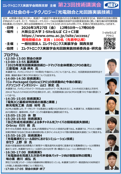
3月27日(金)12時50分~17時00に、エレクトロニクス実装学会 #JIEP 関西支部が第23回技術講演会「AI社会のキーテクノロジー『光電融合と光回路実装技術』」を開催。講演6件。
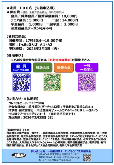
講演会後に名刺交換会。大阪市浪速区・大阪公立大学I-Siteなんばにて。詳細は https://jiep.or.jp/kansai/pdf/2026kansai_technology.pdf に。
#Seminar #CPO #CoPackagedOptics #OpticalPackaging

📡 Stacking GPUs and AI chips with optical circuits for compact design and blazing-fast 114 Tbps bandwidth!
AI semiconductors are evolving with optical-electrical fusion and 3D integration.
• Next-gen Co-Packaged Optics (CPO): “M1000”
• Optical, electrical, and AI chips all packed into a 91mm × 85mm package
• SerDes + PIC + EIC + AI chip — fully stacked

https://xtech.nikkei.com/atcl/nxt/column/18/00001/10660/

#Optoelectronics #Photonics #CoPackagedOptics #AIChips #3DIntegration #PhotonicComputing #semiconductors

光電融合で3D化の波、AI半導体も積層 小型で高速に

 光回路と電気回路を組み合わせた光電融合技術に3D化の波が押し寄せている。GPUやアクセラレーターといったAI半導体を光回路部と積層し、小型化しつつ、高いデータ伝送速度を確保する。早ければ2025年夏ごろに製品化する見込みだ。

日経xTECH