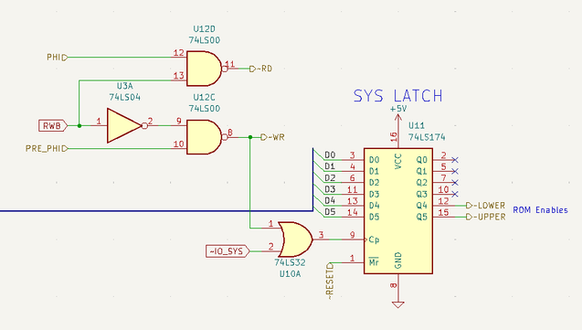
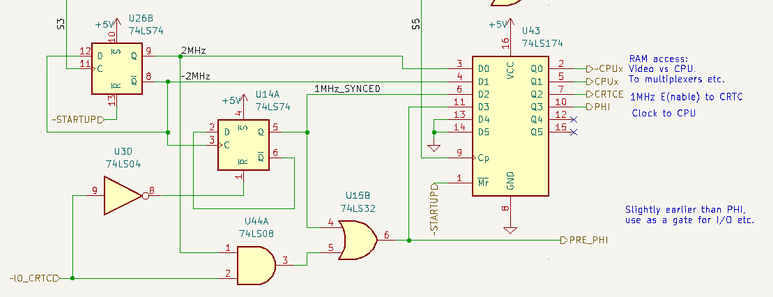
Adding write support to the #mos6502 in the simulator and #CPC_ZERO. The SYS register uses a '174. The clock pulse, to latch the data, could, naively, be driven by a write signal generated by PHI and RWB and gated by ~IO_SEL from the address decoder.
But the 6502 de-asserts RWB at the same moment it releases the data bus. Gate delays would mean the clock pulse arriving after the data bus has been released. Bus capacitance could make this work in the real world but I want proper validation. 1/n