Reinventing PCB Design & Routing with AI: The New Engineering Advantage
The dynamics of modern electronics demand design cycles that are faster, smarter, and significantly more resilient. At Hacktivate Network Solutions, we’re pushing that frontier by integrating AI-driven intelligence into PCB layout, routing, and optimization workflows—unlocking precision and throughput well beyond traditional methods.
Why AI Matters in PCB Design
PCB engineering is no longer just about connecting traces. Today’s boards must balance:
• Increasing layer density
• High-speed signal integrity
• Thermal constraints
• Power distribution accuracy
• EMC/EMI compliance
AI accelerates these constraints into real-time, data-driven decisions—removing hours (or days) of manual iteration.
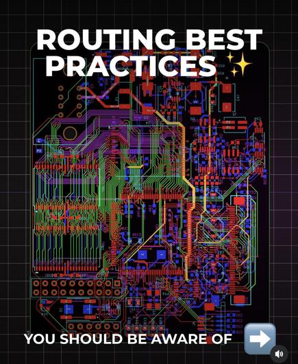
AI-Powered Routing: Speed and Signal Integrity in Sync
Advanced routing engines now leverage machine learning to:
• Predict optimal trace paths based on current density, impedance, and crosstalk patterns
• Auto-correct layout conflicts as the design evolves
• Suggest alternative routing strategies to minimize via usage and reduce layer jumps
• Perform high-speed differential pair tuning automatically
• Optimize copper pours and thermal relief structures with precision
The result: cleaner, more reliable boards with higher electrical performance in a fraction of the time.
Predictive DFM/DFT Intelligence
By training AI on historical fab data, simulated failures, and manufacturability rulesets, designers get instant feedback on:
• Manufacturability risks
• Assembly bottlenecks
• Solder joint failure probability
• Component placement hotspots
• Compliance alignment (IPC, ISO, MIL-STD)
This transforms DFM/DFT from a late-stage check into a proactive design asset.
Closing the Loop with Simulation-Driven Optimization
AI-enhanced digital twins run thermal, electrical, and mechanical simulations continuously. This means:
• Faster validation
• Automated parameter sweeps
• Smarter thermal via placement
• Optimized power integrity profiles
PCB design becomes iterative and adaptive—guided by data, not trial-and-error.
What This Means for Engineering Teams
Organizations adopting AI-supported PCB design gain:
• Shorter development cycles
• Lower NRE and prototype costs
• Higher yield across manufacturing runs
• Better performance on first-pass builds
• Stronger reliability in mission-critical environments
For high-volume manufacturing, defense-grade systems, and enterprise-level hardware deployments, these advantages compound into a decisive competitive edge.
Hacktivate Network Solutions: Engineering at Machine Speed
We integrate AI into every layer of our PCB workflow—from schematic analysis to final routing automation—to deliver boards that are:
• Faster to market
• Built with higher electrical integrity
• Fully optimized for manufacturability and long-term reliability
This is PCB design without constraints—and the future of electronic innovation.