One of the most annoying things in #electronics: you can run a trace under a 0603 resistor, but you can't do that under a 0603 capacitor. The IPC footprints are slightly different, taking the height of the capacitor body into account.

@niconiconi this is one of the reasons I don't include footprints with my auto-generated Altium & KiCad libraries for JLC's parts.
however, I *am* working on a thing that lets you turn their EasyEDA footprints into Altium/KiCad footprints, to get around this annoyance.
@niconiconi no no, I don't mean the standard is annoying!
I have a tool that generates parameterised parts for Altium and KiCad from the JLC parts DB. people often asked why I don't include a footprints library to go with it, and this is one of the reasons - I don't have the height data to generate correct IPC footprints for the parts, so I don't. it's an annoyance in the sense that it'd be nice if I could include footprints.
@niconiconi the parameters are stuff like resistance, power rating, voltage rating, etc. so you can search them easily in your libraries.
the footprint is a convenience thing. drag drop a part into your schematic, and the footprint is already assigned.
the way I do it right now is I just give each component entry a generic footprint name ref, so as long as you have a footprint called "R0402" or whatever it'll use that. but you're responsible for making that to your needs.
@gsuberland @niconiconi there’s also the cases where JLC’s footprints are hilariously wrong (yes, it was a TI power-related part with horrific CAD drawings)
EDIT: TPS55288, https://aus.social/@jpm/114180387563569695
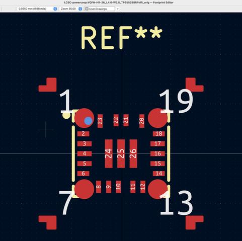
Attached: 1 image It is, however, marginally more correct than JLCPCB's attempt at a footprint for the same part.