Beginnings of a project here. It took an upsetting amount of fiddling around last night to get this working. 1/n
This is my first Pi-based project and I really dislike the complexity and the bulky wiring, but I'm starting to get it under control. I will compactify the layout if it works but for now it's nice to have access to everything. 2/n
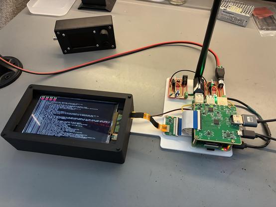
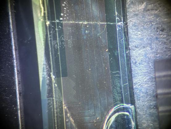
Anyway this slow-moving project is a little photolithography setup for making PCBs at home. No need to remind me that it's probably not worth the trouble … the journey is the destination and I'm leaning a lot. For example I learned that I need to be more gentle when removing the LCD panel's backlight because I cracked this one and broke all the traces from the flex cable. 3/n
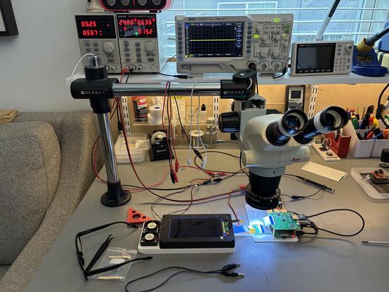
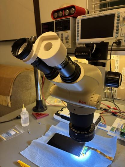
I made an iPhone adapter for my microscope so I could take a photo of the damage (the narrow traces are about 20µ across, it's nuts). 4/n
I ordered a replacement LCD that was pre-modded with backlight removed and tempered glass affixed to the top (sold as an SLA printer part). Seems to work but I don't know how much UV is making it through. Will need to do some experiments. Anyway, progress! 5/n
Did a bunch of experiments and it seems that my LCD is opaque to the 365nm lamp I’m using. I randomly have a 405nm lamp from a free pile so I’ll see if that one works. Chemistry is hard. 6/n
@tpolecat
What do you think would be faster? Create a schematic and PCB layout and order new flex from China or repair the broken traces?
What do you think would be faster? Create a schematic and PCB layout and order new flex from China or repair the broken traces?
@maker_tom Oh, repairing them is hopeless, they’re microscopic and bonded to glass. I ordered a new one. It’s a $25 part so not the end of the world. I’ll be more careful next time.