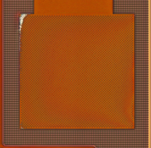
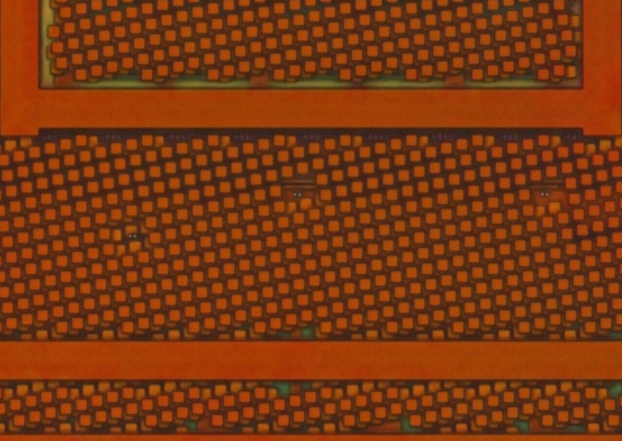
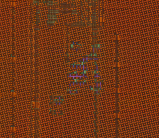
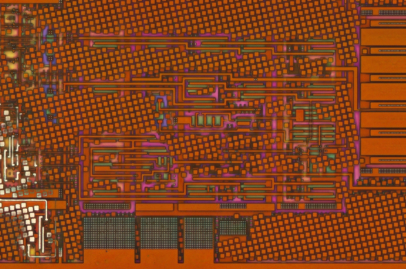
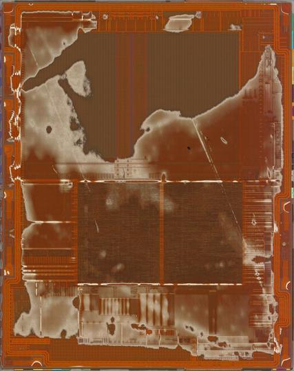
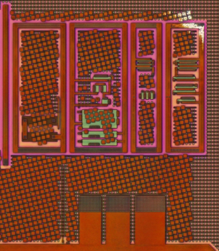
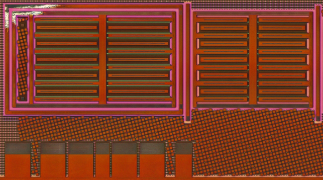
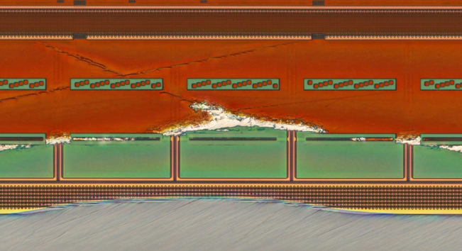
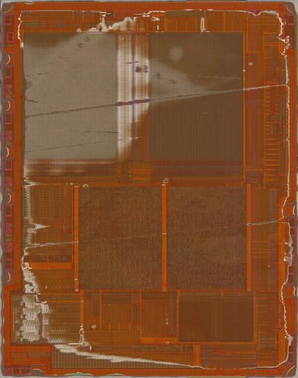
This was for the lapping experiment no.2. I am and will be taking images of every step e.g. when I hit a layer. This is around an hour of lapping work and ~18 hours of imaging the result. So one layer per day if I do everything well unlike yesterday, lol.

See alt text for description.

#reverseengineering

A pad structure including an array of vias to the layer below, visible here as bright dots.
Sporadically, there are more vias in groups of two. These contact the mesh on top metal.
Finally, I just like how this looks. A glimpse through three more metal layers.
Going down further, metal-3 is half gone. Here is what metal-2 and below looks like. Vias are again clearly identifiable.

Now, that one's done imaging and stitching. I've lapped it down to remove the rest of this metal layer already, imaging it comes next...

Can already tell the top array is EEPROM/Flash. A couple more memories appear to be in the bottom as well.

Now only M1 and M2 in the sea of gates..

Full die with M2 and below. Some M2 started to peel on the perimeter, and a little bit of M3 remains over the sea of gates. I thought I'd rather shoot this one than keep lapping further.

Now I can ID the memory blocks at the bottom; three SRAM arrays of different sizes and a block of ROM it seems, which is the rightmost one.

I/O pad circuitry with only M1 remaining.

Three distinct blocks are there, logic circuitry, medium-drive transistors, and tow high-drive transistors for driving the pad. For standard cells, M1 seems to be solely for power delivery and local interconnect, inter-cell routing is on M2 and higher layers. Interesting to see the substrate colour changes based on the doping type; pink and green. Pink seems to have smaller FETs on average, so I'm inclined to say this is the N-type.

For comparison, here is another pad type. Here, there is no small-power logic present, at all. Fewer transistors in the medium-drive section. Power FETs were turned into ESD protection diodes: no gate connection. And only a single wire running down to the rest of the chip.
Here is the answer re what's under all that power distribution routing around the chip. Capacitors. Vias through the opening go from poly to upper metal, vias on the perimeter go to M1.
Another full die imaging run, with M2 getting stripped. Scratched slightly; I think only M2 is damaged though.

And another, with more of M2 removed.

EDIT: Fixed threading.

Aaaand I lost the sample. :D

/๐Ÿงต

SAMPLE RECOVERED! The thread shall be resumed soon, stand by.