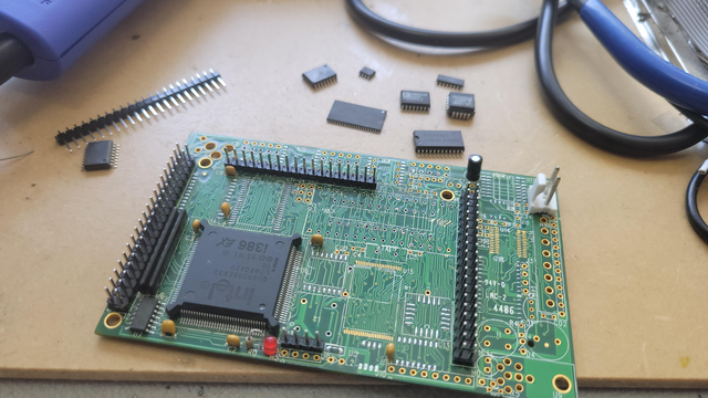
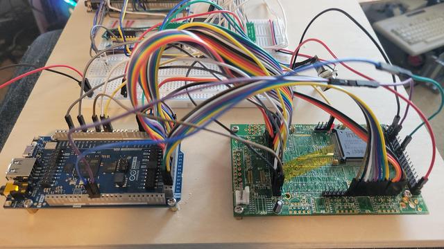
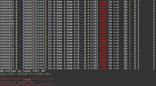
Ok, starting a new thread cuz the last one is old. Since my 286 CPU appears to be dead, I figured while I wait on my next order of 80C286 chips from eBay I thought I'd work on the 386EX board.

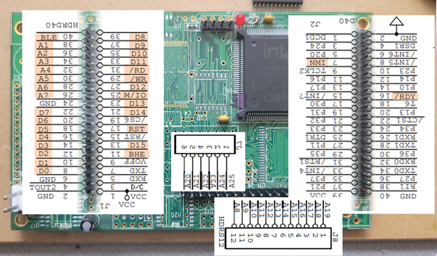
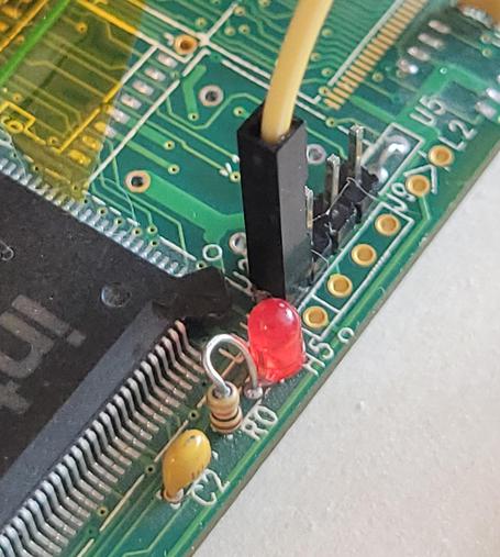
Here's where we're at, with the board stripped of components and headers soldered on.

#retrocomputing #arduino

Almost every pin I need is accessible via the headers - except one, and its one I kinda need. It's the D/C or Data/Code pin. The 386 no longer emits an octal bus status like the Intel chips before it did; instead it emits bus signals directly.

The Data/Code pin tells us whether the current bus operation read is just reading memory or fetching code. That's important if we're going to feed the CPU instructions.

It's not strictly required if we just emulate memory, but its nice to have as just feeding the CPU code bytes when it is fetching is convenient as the address doesn't matter.

If we're going to make 386 tests as well, this is an important pin to capture the state of for that purpose.

Without a schematic I can't really see if the D/C pin actually goes anywhere. It has a pad, but no trace on the top layer. That doesn't mean it's not connected somewhere, but you've got a dumb cow here not Tube Time.

They wouldn't really have needed it to build this board. There's no reason to concern the SRAM with whether its serving up code or data. So likely it just goes nowhere.

So that means I have to solder a wire to this...

Let's make sure we absolutely have the right pin.

A good sanity check is that VSS connects to at thick ground copper, and M/IO connects to a via, that we can trace out going to the correct header pin.

*sweating*

OK, without any clock source this thing should barely draw any power.

Half a watt seems about right. Much more reassuring than the 286 was!

This is a 3V capable CPU though, so we'll run the board at 3V. It draws 0.1 W at 3.3V which is even better.

Still wondering what happened to my 80C286. Wish I had a system I could throw it in to see if it was actually dead or if I'm just a bonehead.

here's what i have to patch over to the Arduino

50% chance i have one or both of the address headers backwards lol

This should be it! It's the same gpio pinout as the 286 basically. The 386EX actually only has two more address lines. I guess 64MB of RAM is plenty for embedded applications...
Lucky that this header just happens to have CLK on it.
Conspicuously absent on the 386 is an ALE pin. I guess timings are now tight enough that you only concern yourself with the address when a read or write signal is asserted.
No bus status, no ALE pin... I guess I know the CPU has reset if it just reads something.

And I thought the 286 took a long time to reset.

450 cycles!

So far no response from the 386EX.

Time to do a sanity check to determine whether the RESET and CLK signals are really reaching the CPU.

The header provides a tie to /RST, that is an inverted RESET signal. This is one of the signals that passes through the inverter IC, a 74HC14D. I should check that the inverter is still receiving power after my board surgery, and that a positive RESET signal is coming out the other end of it.
Well, this is unfortunate. The holes in the board i assumed were for mounting posts actually seem to be connected to each plane and by putting screws in I have shorted the board.

The EX datasheet doesn't mention the particulars, but the SX datasheet has this to say:

I'm not sure how this board ties the busy pin. If it isn't low we're gonna be waiting a million cycles for it to reset.

BUSY is multiplexed with TMRGATE2 on Pin 92. It looks like this runs through a resistor network with a pulldown to ground (figures) but does go to a header pin curiously claled TMRCLK2. Typo perhaps? I hope so.