 Kevin's Blog
Watching a Z80 from an RP2350
I’m messing around with the Raspberry Pi Pico RP2350 and PIO and at some point want to see if I can hook it up to a Z80.
As a starter, I’ve been experimenting with seeing if I can get an RP2350 to see the Z80 address and data bus in any manner.
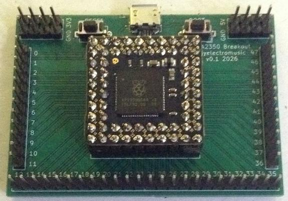
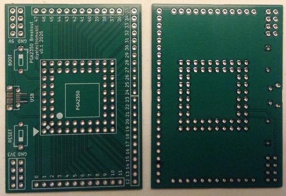
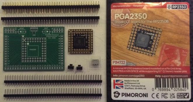
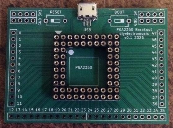
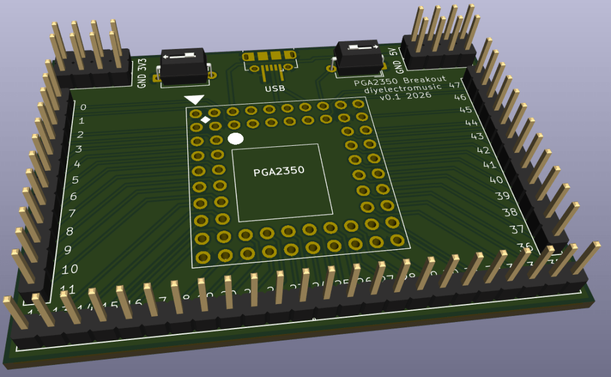
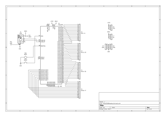
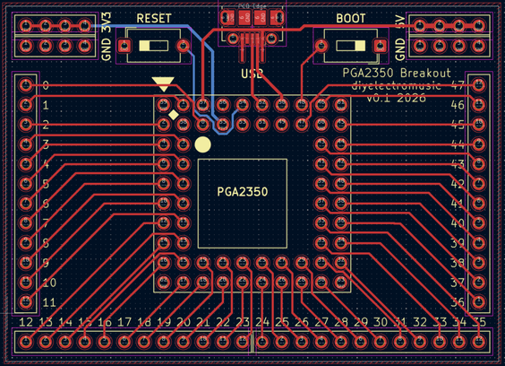
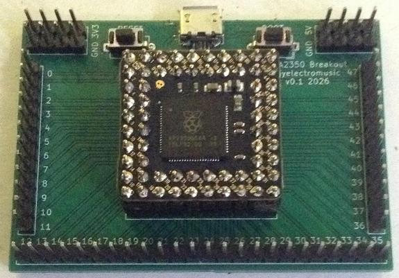
I’m using a Pimoroni PGA2350 in my own custom breakout PCB.
https://makertube.net/w/vPwqyBG8s5XBZzN3Zwwfrz
The Z80 Bus
There is a lot of detail out there about the Z80 and Z80 bus, so I’m not going to go over that again here, but here are some key references:
- http://www.z80.info/ – the home of everything Z80!
- The RC2014 bus specification and description.
- Electronic Circuits – interfacing with a Z80 microprocessor v3 (data and address buses).
- Z80 User Manual – Chapter on “Timing”.
- Build Your Own Z80 Computer – Steve Ciarcia
The key features relevant to me are:
- 16-bit address bus (A0-A15).
- 8-bit data bus (D0-D7).
- A number of OUTPUT control lines.
- A number of INPUT control lines (including RESET and CLOCK).
The original Z80 was an NMOS device and ran at 2.5MHz (Z80), but there were 4MHz (Z80A) and 6MHz (Z80B) versions soon afterwards. Then the CMOS versions appeared with a whole range of clock speeds, typically 8MHz (Z84C0008) and 10MHz (Z84C0010), and even up to 20MHz (Z84C0020). They were made by a whole host of different manufacturers – Zilog, SGS, ST, NEC, Mostek, etc (more here), but they don’t all seem to have had the same numbering schemes that I could find.
It was discontinued in 2024, although some overseas marketplaces assure me that they can provide brand new 20MHz Zilog Z84C0020’s at less than a few £s each 😉
A Z80 CPU Tester will give an idea of the type and speed of any unknown Z80 found “in the wild” though (I had fun testing a batch of said “20MHz” devices myself).
The Z80 Clock
Of particular interest to me is the clock speed. In particular, what is the minimum clock speed possible? There are some (modern, apparently) versions of the Z80 that are fully static – i.e. they will retain state between clock pulses, including a complete stop. But I’m not clear if most are. But seeing as someone managed to create a hand-cranked, clocked Z80 based computer, I suspect a really slow clock is unlikely to be an issue. There is a note here that it is best to hold the clock HIGH when not being cycled.
Going back to the original Z80A datasheet, we find:
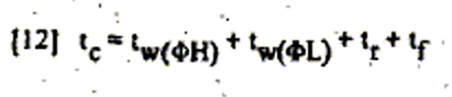
The max clock period is defined in note [12] as:
So basically adding those values together. The max pulse width for LOW has a given value of 2000nS, and the rise and fall times are fixed at 30nS, so key to determining the longest period accepted is the max pulse width for HIGH. That is provided in note [E]:
So the implication is that clock LOWs should be no longer than 2uS, but clock HIGHs in principle can be anything, with guaranteed functionality up to 200uS. This gives a total clock period of at least around 203uS which equates to a clock frequency of just under 5KHz.
This explains the previous noted comment about holding clocks HIGH.
One issue could be that some signals need several clock cycles. In particular, RESET is expected to be held for 3 clock cycles to ensure a proper reset occurs, so that will naturally have to be longer for longer clock pulses.
It is worth noting at this point that the Z80 has two concepts of a cycle: machine (M) cycles and clock (T) cycles (sometimes called states). Machine cycles are multiples of clock cycles (typically 3 to 6 T cycles per M cycle). Many Z80 instruction references will list the number of cycles (M) and states (T) that an instruction will take to execute.
There is also the option for an external peripheral (e.g. memory) to get the Z80 CPU to wait. This involves asserting the /WAIT signal until the peripheral is ready to continue. This allows synchronisation between the CPU and slower memory.
Part of the consequence of all this is that a single-clock-cycling option isn’t particularly useful, as it will need several steps of the single-cycle clock to execute a single Z80 instruction.
For interest, there is an instruction-aware single-stepper circuit in the Build Your Own Z80 Computer book (figure 4.5), which can monitor /M1 and use /WAIT to pause the CPU until the next step.
RP2350 GPIO
I’m using the Arduino Pico core from here: https://github.com/earlephilhower/arduino-pico
Which makes it easy to build and download code to the RP2350, but I’m trying to stick to Pico C/C++ SDK functions rather than using the Arduino environment overlays.
To initialse GPIO on an RP2040/RP2350 requires the following:
gpio_init(pin);gpio_set_dir(pin, dir);
gpio_put(pin, value);
value = gpio_get(pin);
But this is too slow for a bus read. But there is an option to act on several GPIO pins at the same time, for example:
gpio_init_mask(gpiobitmap);gpio_set_dir_in_masked(gpiobitmap);
gpio_clr_mask(gpio_bitmap);
gpio_set_mask(gpio_bitmap);
uint32_t value = gpio_get_all();
But these APIs were designed with the RP2040 in mind, and so only needs to address up to 32 GPIO pins. The RP2350B I’m using has 48 GPIO, so the SDK has the concept of a GPIO base, which can be 0 (for the range 0-31) or 1 (for the range 32-63).
Unfortunately how this appears in the API is a little inconsistent. In some cases there is a _n version of the API which takes a base (0 or 1) as a parameter. In some cases, e.g. for single GPIO pins, any value up to the maximum supported is fine.
PIO is different again and the base needs to be set before hand using pio_set_gpio_base. But for PIO the base is treated differently: base 0 is GPIO 0-31, but base 1 is GPIO 16-47. I guess this is to allow a fully parallel 32 GPIO pins in both cases, but it is confusing being different to the non-PIO functions.
Some API functions don’t have an equivalent (that I could find anyway), so I could find no “base 1” version of gpio_init_mask.
To initialise all the GPIO I need uses the following:
gpio_init_mask(GP_BASE0_MASK);gpio_set_dir_in_masked(GP_BASE0_MASK);
for (int i=0; i<GP_LED_PINS; i++) {
gpio_init(ledPins[i]);
gpio_set_dir(ledPins[i], true); // out = true
}
I also find it really annoying that there are gpio_set_dir_in/out functions for combinations of pins, but for a single pin you have to use gpio_set_dir(pin, direction) where direction is a bool indicating out or not.
RP2350 Test Code
The simplest code will take what is received on the Z80 data bus and write it straight out to some LEDs. This is what is going on in the following code.
Note this is NOT real-time – it is just a continually updating snapshot of the data bus, not an accurate representation of the full activity and certainly not synchronised to any of the bus control signals.
In short, it looks pretty, but is essentially useless for any practical purposes. But it illustrates the idea and shows the connections are working.
// GPIO Base 0 Definitions// Start from GPIO 0 up to GPIO 31
//
#define GP_ADDR_START 0ul
#define GP_ADDR_PINS 16ul
#define GP_ADDR_MASK (0xFFFFul<<GP_ADDR_START)
#define GP_DATA_START 16ul
#define GP_DATA_PINS 8ul
#define GP_DATA_MASK (0xFFul<<GP_DATA_START)
#define GP_RD 24ul
#define GP_WR 25ul
#define GP_M1 28ul
#define GP_MREQ 30ul
#define GP_IORQ 31ul
#define GP_CTRL_MASK ((1ul<<GP_RD)|(1ul<<GP_WR)|(1ul<<GP_M1)|(1ul<<GP_MREQ)|(1ul<<GP_IORQ))
#define GP_CTRL_PINS 5ul
int ctrlPins[GP_CTRL_PINS] = {GP_RD, GP_WR, GP_M1, GP_MREQ, GP_IORQ};
#define GP_BASE0_MASK (GP_ADDR_MASK | GP_DATA_MASK | GP_CTRL_MASK)
// GPIO Base 1 Definitions
// Start from GPIO 32 onwards
//
#define GP_LED_START 40
#define GP_LED_MASK (0xFF<<(GP_LED_START-32))
#define GP_LED_PINS 8
int ledPins[GP_LED_PINS] = {40,41,42,43,44,45,46,47};
#define GP_BASE1_MASK (GP_LED_MASK)
void setup() {
// Pins in range lower than 32 can be initialised at once
gpio_init_mask(GP_BASE0_MASK);
gpio_set_dir_in_masked(GP_BASE0_MASK);
// Set the LED outputs
// Can't be set all at once I think...
for (int i=0; i<GP_LED_PINS; i++) {
gpio_init(ledPins[i]);
gpio_set_dir(ledPins[i], true); // out = true
}
}
void loop() {
uint32_t gpio31 = gpio_get_all();
uint8_t data8 = (GP_DATA_MASK & gpio31) >> GP_DATA_START;
gpio_clr_mask_n(1, GP_LED_MASK);
gpio_set_mask_n(1, (data8<<(GP_LED_START-32)));
delay(5);
}
RC2350 8-bit IO Module
Having got this far, it is now possible to check for various control values on the Z80 bus, for example perhaps looking for an IO write to a certain address.
For an IO write, I need to look for /IORQ and /WR going LOW and then the address I’m interested in appearing in the lower 8 bits of the address bus. Then I can pull the data off the data bus.
The following code looks for a write to IO address 0 and lights the LEDs according to the value of the data bus.
void loop() {uint32_t gpio32 = gpio_get_all();
// Look for /IORQ, /WR, and ADDR matching IO location 0
if (
((gpio32 & GP_CTRL_MASK) == ((1<<GP_RD)|(0<<GP_WR)|(1<<GP_M1)|(1<<GP_MREQ)|(0<<GP_IORQ)))
&& ((gpio32 & 0xFF) == 0)
)
{
// Grab the data off the bus and update LEDs
uint8_t data8 = (GP_DATA_MASK & gpio32) >> GP_DATA_START;
gpio_clr_mask_n(1, GP_LED_MASK);
gpio_set_mask_n(1, (data8<<(GP_LED_START-32)));
}
}
I’ve basically used a 32-bit dual-core ARM CORTEX M0+ running at 150MHz to emulate a couple of TTL logic chips as can be found in the RC2014 digital IO module to flash some LEDs from an 8-bit, 10MHz processor!
This is the BASIC code that is running on the RC2014:
10 FOR F=1 TO 620 OUT 0,2^F
30 GOSUB 100
40 NEXT F
50 FOR F=7 TO 0 STEP -1
60 OUT 0,2^F
70 GOSUB 100
80 NEXT F
90 GOTO 10
100 FOR Z=1 TO 200
110 NEXT Z
120 RETURN
You can see this running in the video at the start of this post.
Conclusion
Naturally this is a pretty crazy thing to be doing, but it is showing the basic idea.
At present, this is just running at full CPU speed, consuming one of the cores of the RP2350 just to watch what is going on, on the bus.
There are a number of interesting directions that could now be taken. Some that I’m pondering are:
- Support both read and write, i.e. INPUT and OUTPUT IO access.
- Getting the IO handling onto one core of the RP2350 whilst the other core does something with the information.
- A memory-mapped device, watching for memory reads and writes.
- Controlling the Z80 clock from the RP2350 for some interesting clock control possibilities – varying speeds, instruction aware-stepping, etc.
- Go back to my experiments with PIO on the Raspberry Pi Pico to see if I can do it more autonomously.
- Emulate some of the existing Z80 peripherals, similar to how the Pico is used on the RP6502 The Picocomputer. Although it is worth noting that this is essentially what the Z80-MBC is doing…
I doubt many of these will get past the thinking stage, but there are a lot of options now the basic mechanisms seem to work.
Kevin
#pga2350 #rc2014 #rp2350 #z80

 diyelectromusic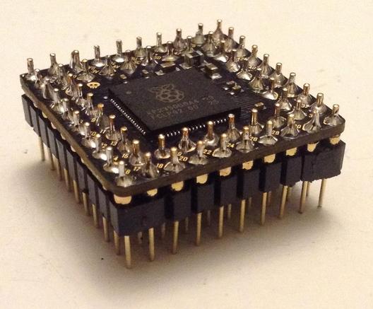
 Simple DIY Electronic Music Projects